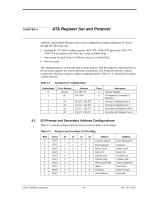
SanDisk SDCFB-64-A10 Product Manual - Page 48
True IDE Mode Addressing, ATA Registers
 |
UPC - 619659015190
View all SanDisk SDCFB-64-A10 manuals
Add to My Manuals
Save this manual to your list of manuals |
Page 48 highlights
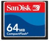
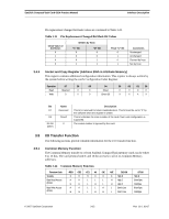
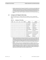
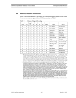
ATA Register Set and Protocol SanDisk CompactFlash Card OEM Product Manual 4.4 True IDE Mode Addressing When a CompactFlash Memory Card is configured in the True IDE Mode the I/O decoding is as listed in Table 4-5. Table 4-5 True IDE Mode I/O Decoding -CE2 -CE1 A2 A1 A0 -IORD=0 1 0 0 0 0 Even RD Data 1 0 0 0 1 Error Register 1 0 0 1 0 Sector Count 1 0 0 1 1 Sector No. 1 0 1 0 0 Cylinder Low 1 0 1 0 1 Cylinder High 1 0 1 1 0 Select Card/Head 1 0 1 1 1 Status 0 1 1 1 0 Alt Status 0 1 1 1 1 Drive Address -IOWR=0 Even WR Data Features Sector Count Sector No. Cylinder Low Cylinder High Select Card/Head Command Device Control Reserved 4.5 ATA Registers In accordance with the PCMCIA specification: each of the registers below which is located at an odd offset address may be accessed at its normal address and also the corresponding even address (normal address -1) using data bus lines (D15-D8) when -CE1 is high and -CE2 is low unless -IOIS16 is high (not asserted) and an I/O cycle is being performed. 4.5.1 Data Register (Address-1F0[170]; Offset 0, 8, 9) The Data Register is a 16-bit register, and it is used to transfer data blocks between the CompactFlash Memory Card data buffer and the host. This register overlaps the Error Register. The information in Table 3-6 describes the combinations of data register access and is provided to assist in understanding the overlapped Data Register and Error/Feature Register rather than attempt to define general PCMCIA word and byte access modes and operations. Refer to the PCMCIA PC Card Standard Release 2.0 for definitions of the Card Accessing modes for I/O and memory cycles. NOTE: Because of the overlapped registers, access to the 1F1, 171 or offset 1 are not defined for word (-CE2 = 0 and -CE1 = 0) operations. SanDisk products treat these accesses as accesses to the Word Data Register. The duplicated registers at offsets 8, 9 and Dh have no restrictions on the operations that can be performed by the socket. Table 4-6 Data Register Data Register Word Data Register Even Data Register Odd Data Register Odd Data Register Error/Feature Register CE2- CE1- A0 0 0 X 1 0 0 1 0 1 0 1 X 1 0 1 Offset 0,8,9 0,8 9 8,9 1,Dh Data Bus D15-D0 D7-D0 D7-D0 D15-D0 D7-D0 02/07, Rev. 12.0 4-4 © 2007 SanDisk Corporation
-
 1
1 -
2
-
3
-
4
-
5
-
6
-
7
-
8
-
9
-
10
-
11
-
12
-
13
-
14
-
15
-
16
-
17
-
18
-
19
-
20
-
21
-
22
-
23
-
24
-
25
-
26
-
27
-
28
-
29
-
30
-
31
-
32
-
33
-
34
-
35
-
36
-
37
-
38
-
39
-
40
-
41
-
42
-
 43
43 -
 44
44 -
 45
45 -
 46
46 -
 47
47 -
 48
48 -
 49
49 -
 50
50 -
 51
51 -
 52
52 -
 53
53 -
54
-
55
-
56
-
57
-
58
-
59
-
60
-
61
-
62
-
63
-
64
-
65
-
66
-
67
-
68
-
69
-
70
-
71
-
72
-
73
-
74
-
75
-
76
-
77
-
78
-
79
-
80
-
81
-
82
-
83
-
84
-
85
-
86
-
87
-
88
-
89
-
90
-
91
-
92
-
93
-
94
-
95
-
96
-
97
-
98
-
99
-
100
-
101
-
102
-
103
-
104
-
105
-
106
-
107
-
108
 |
 |