SanDisk SDCFH-4096 Product Manual - Page 32
Common and Attribute Memory Write Timing Diagram
 |
UPC - 814227015149
View all SanDisk SDCFH-4096 manuals
Add to My Manuals
Save this manual to your list of manuals |
Page 32 highlights
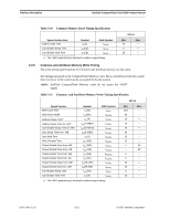
Interface Description SanDisk CompactFlash Card OEM Product Manual Figure 3-4 Common and Attribute Memory Write Timing Diagram NOTE 1: NOTE 2: NOTE 3: NOTE 4: Shaded areas may be high or low. When the data I/O pins are in the output state, no signals shall be applied to the data pins (D[15::0]) by the host system May be high or low for write timing, but restrictions on -OE from previous figures apply. SanDisk CompactFlash Memory Cards do not assert the -WAIT signal. 02/07, Rev. 12.0 3-14 © 2007 SanDisk Corporation
-
 1
1 -
2
-
3
-
4
-
5
-
6
-
7
-
8
-
9
-
10
-
11
-
12
-
13
-
14
-
15
-
16
-
17
-
18
-
19
-
20
-
21
-
22
-
23
-
24
-
25
-
26
-
 27
27 -
 28
28 -
 29
29 -
 30
30 -
 31
31 -
 32
32 -
 33
33 -
 34
34 -
 35
35 -
 36
36 -
 37
37 -
38
-
39
-
40
-
41
-
42
-
43
-
44
-
45
-
46
-
47
-
48
-
49
-
50
-
51
-
52
-
53
-
54
-
55
-
56
-
57
-
58
-
59
-
60
-
61
-
62
-
63
-
64
-
65
-
66
-
67
-
68
-
69
-
70
-
71
-
72
-
73
-
74
-
75
-
76
-
77
-
78
-
79
-
80
-
81
-
82
-
83
-
84
-
85
-
86
-
87
-
88
-
89
-
90
-
91
-
92
-
93
-
94
-
95
-
96
-
97
-
98
-
99
-
100
-
101
-
102
-
103
-
104
-
105
-
106
-
107
-
108
 |
 |
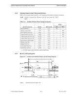
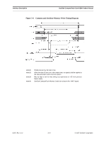
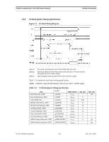
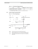
Interface Description
SanDisk CompactFlash Card OEM Product Manual
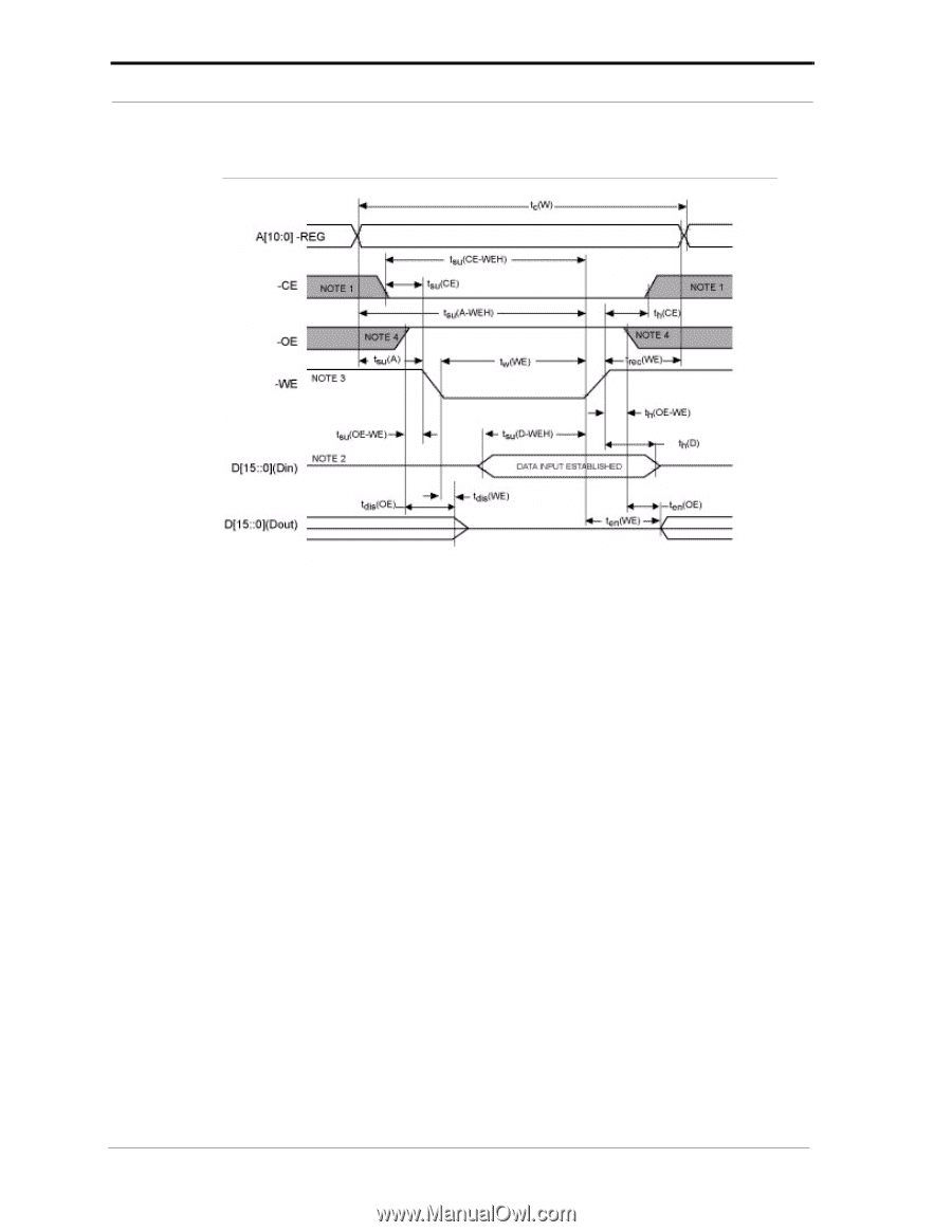
Figure 3-4
Common and Attribute Memory Write Timing Diagram
NOTE
1:
Shaded areas may be high or low.
NOTE
2:
When the data I/O pins are in the output state, no signals shall be applied to
the data pins (D[15::0]) by the host system
NOTE
3:
May be high or low for write timing, but restrictions on -OE from previous
figures apply.
NOTE
4:
SanDisk CompactFlash Memory Cards do not assert the -WAIT signal.
02/07, Rev. 12.0
3-14
© 2007 SanDisk Corporation