SanDisk SDCFX3-004G-bulk Product Manual - Page 29
Power Up/Power Down Timing for Systems not supporting RESET, Table 3-10, Common Memory - tv
 |
UPC - 809905301577
View all SanDisk SDCFX3-004G-bulk manuals
Add to My Manuals
Save this manual to your list of manuals |
Page 29 highlights
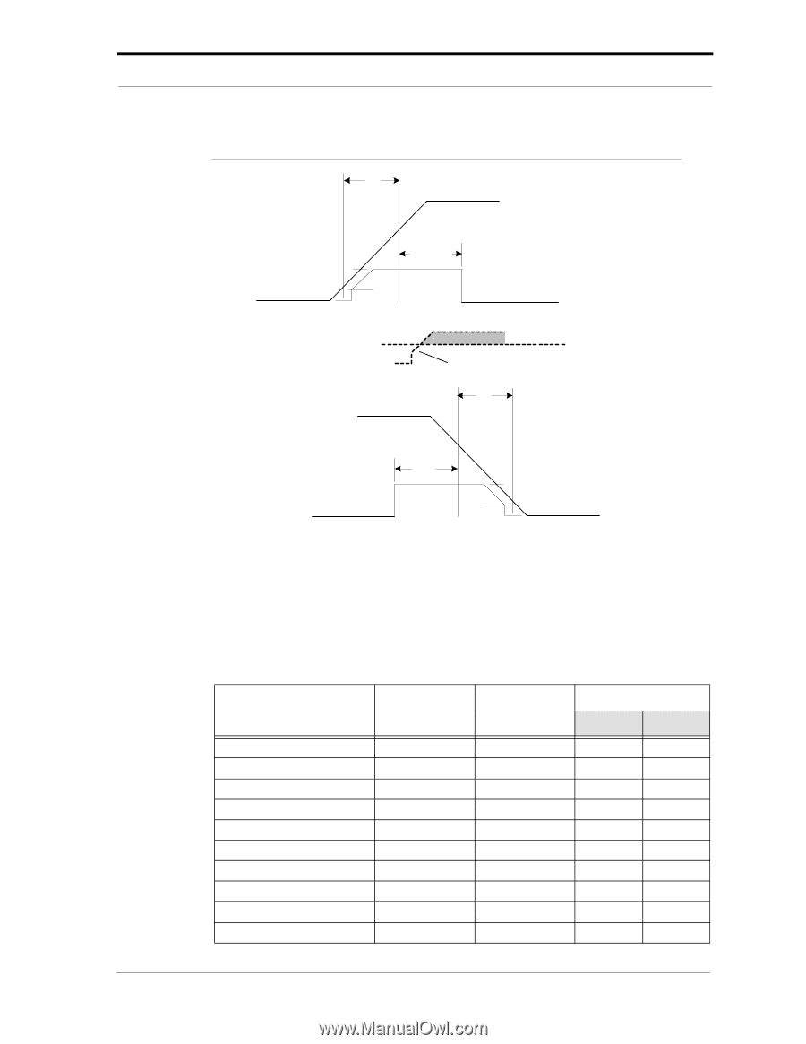
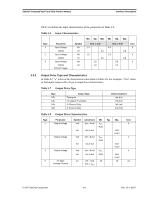
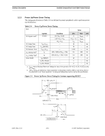
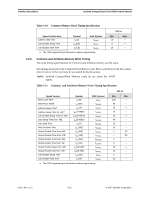
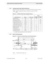
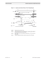
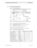
SanDisk CompactFlash Card OEM Product Manual Interface Description Figure 3-2 Power Up/Power Down Timing for Systems not supporting RESET tpr VCC Min. VIH tSU(VCC) 2V VCC -CE1, -CE2 Always Hi-z from system RESET VCC -CE1, -CE2 Supplied by pull-up resistor on card (if present) tpf VCC Min. trec VIH 2V 3.3.4 Common Memory Read Timing Table 3-10 contains common memory read timing specifications for all types of memory. NOTE: All timings measured at the CompactFlash Memory Card. Skews and delays from the system driver/receiver to the card must be accounted for by the system. Table 3-10 Common Memory Read Timing Specification Speed Version Item Read Cycle Time Address Access Timea Card Enable Access Time Output Enable Access Time Output Disable Time from -OE Output Disable Time from -CE Output Enable Time from -CE Output Enable Time from -OE Data Valid from Add Changea Address Setup Time Symbol tc (R) ta (A) ta (CE) ta (OE) tdis (OE) tdis (CE) ten (CE) ten (OE) tv (A) tsu (A) IEEE Symbol tAVAV tAVQV tELQV tGLQV tGHQZ tEHQZ tELQNZ tGLQNZ tAXQX tAVGL 100 ns Min. 100 ----------- 5 5 0 10 Max. --100 100 50 50 50 --------- © 2007 SanDisk Corporation 3-11 Rev. 12.0, 02/07
-
 1
1 -
2
-
3
-
4
-
5
-
6
-
7
-
8
-
9
-
10
-
11
-
12
-
13
-
14
-
15
-
16
-
17
-
18
-
19
-
20
-
21
-
22
-
23
-
 24
24 -
 25
25 -
 26
26 -
 27
27 -
 28
28 -
 29
29 -
 30
30 -
 31
31 -
 32
32 -
 33
33 -
 34
34 -
35
-
36
-
37
-
38
-
39
-
40
-
41
-
42
-
43
-
44
-
45
-
46
-
47
-
48
-
49
-
50
-
51
-
52
-
53
-
54
-
55
-
56
-
57
-
58
-
59
-
60
-
61
-
62
-
63
-
64
-
65
-
66
-
67
-
68
-
69
-
70
-
71
-
72
-
73
-
74
-
75
-
76
-
77
-
78
-
79
-
80
-
81
-
82
-
83
-
84
-
85
-
86
-
87
-
88
-
89
-
90
-
91
-
92
-
93
-
94
-
95
-
96
-
97
-
98
-
99
-
100
-
101
-
102
-
103
-
104
-
105
-
106
-
107
-
108
 |
 |