Seagate ST39204LC Product Manual - Page 78
Cheetah 18XL Product Manual, Rev. G, Input characteristics
 |
View all Seagate ST39204LC manuals
Add to My Manuals
Save this manual to your list of manuals |
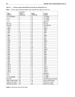
Page 78 highlights
68 Cheetah 18XL Product Manual, Rev. G The output characteristics shall additionally conform to EIA RS-485. STEADY STATE LOGIC INPUT (1 OR 0) D -SIGNAL 100Ω V1 Vs 75Ω +SIGNAL 100Ω V2 Figure 24. LVD output signals MEASURED PARAMETER DEVICE CONNECTOR Input characteristics Each signal (Vs) received by LVD interface receiver circuits shall have the following input characteristics when measured at the disk drive connector: Steady state Low level output voltage* = 0.030 V = < Vs = < 3.6 V (signal negation/logic 0) Steady state High level output voltage* = -3.6 V = < Vs = < -0.030 V (signal assertion/logic 1) Differential voltage = +0.30 V minimum with common-mode voltage ranges 0.700 V = < Vcm = < 1.800 V. (X3T10/1302D) *These voltages shall be measured between the output terminal and the SCSI device's logic ground reference. Input characteristics shall additionally conform to EIA RS-485-983. Single Ended Circuitry VCCA LVD Signal Drivers LVD Receiver VCCB Single Ended Receiver Single Ended Negation Driver Single Ended Ground Driver LVD Signal Drivers Ground Single Ended: GND LVD: +Signal -Signal -Signal Figure 25. Typical SE-LVD alternative transmitter receiver circuits Single Ended Assertion Driver
-
 1
1 -
2
-
3
-
4
-
5
-
6
-
7
-
8
-
9
-
10
-
11
-
12
-
13
-
14
-
15
-
16
-
17
-
18
-
19
-
20
-
21
-
22
-
23
-
24
-
25
-
26
-
27
-
28
-
29
-
30
-
31
-
32
-
33
-
34
-
35
-
36
-
37
-
38
-
39
-
40
-
41
-
42
-
43
-
44
-
45
-
46
-
47
-
48
-
49
-
50
-
51
-
52
-
53
-
54
-
55
-
56
-
57
-
58
-
59
-
60
-
61
-
62
-
63
-
64
-
65
-
66
-
67
-
68
-
69
-
70
-
71
-
72
-
 73
73 -
 74
74 -
 75
75 -
 76
76 -
 77
77 -
 78
78 -
 79
79 -
 80
80 -
 81
81 -
 82
82 -
 83
83 -
84
-
85
-
86
-
87
-
88
-
89
-
90
-
91
-
92
-
93
-
94
 |
 |
