Sony 1000RF Service Manual - Page 2

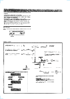
SERVICE NOTE, Printed Wiring Boards -CD Mechanism

Page 2 highlights

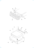
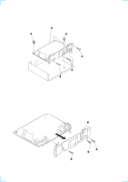
SERVICE NOTE CAUTION Use of controls or adjustments or performance of procedures other than those specified herein may result in hazardous radiation exposure. Notes on Chip Component Replacement • Never reuse a disconnected chip component. • Notice that the minus side of a tantalum capacitor may be dam- aged by heat. NOTES ON HANDLING THE OPTICAL PICK-UP BLOCK OR BASE UNIT The laser diode in the optical pick-up block may suffer electrostatic breakdown because of the potential difference generated by the charged electrostatic load, etc. on clothing and the human body. During repair, pay attention to electrostatic breakdown and also use the procedure in the printed matter which is included in the repair parts. The flexible board is easily damaged and should be handled with care. NOTES ON LASER DIODE EMISSION CHECK The laser beam on this model is concentrated so as to be focused on the disc reflective surface by the objective lens in the optical pickup block. Therefore, when checking the laser diode emission, observe from more than 30 cm away from the objective lens. NOTES ON PICK-UP FLEXIBLE BOARD The pick-up flexible board in this set is secured to the optical pickup with an adhesive tape. Once the tape is removed, an adhering force becomes weak, and it cannot be reused. Therefore, if the optical pick-up is replaced, replace also the pickup flexible board with a new one. SAFETY-RELATED COMPONENT WARNING!! COMPONENTS IDENTIFIED BY MARK 0 OR DOTTED LINE WITH MARK 0 ON THE SCHEMATIC DIAGRAMS AND IN THE PARTS LIST ARE CRITICAL TO SAFE OPERATION. REPLACE THESE COMPONENTS WITH SONY PARTS WHOSE PART NUMBERS APPEAR AS SHOWN IN THIS MANUAL OR IN SUPPLEMENTS PUBLISHED BY SONY. TABLE OF CONTENTS 1. GENERAL Location of controls 3 Getting Started 3 Operation 3 Connections 4 2. DISASSEMBLY 2-1. Panel Assy, Front 5 2-2. CD Mechanism Block 5 2-3. Main Board 6 2-4. Chassis (Rear 6 2-5. Chassis (T) Sub Assy 7 2-6. Lever Assy 7 2-7. Servo Board 8 2-8. Roller Assy 8 2-9. Chassis (OP) (O/S) Assy 9 2-10. Optical Pick-up Block 9 3. ELECTRICAL ADJUSTMENTS CD Section 10 4. DIAGRAMS 4-1. IC Pin Description 11 4-2. Block Diagram -CD Section (1/2 12 4-3. Block Diagram -CD Section (2/2 13 4-4. Block Diagram -Display, Power Supply Section 14 4-5. Circuit Boards Location 15 4-6. Printed Wiring Boards -CD Mechanism Section 16 4-7. Schematic Diagram -CD Mechanism Section 17 4-8. Printed Wiring Board -Main Section 18 4-9. Schematic Diagram -Main Section (1/2 19 4-10. Schematic Diagram -Main Section (2/2 20 4-11. Schematic Diagram -Display Section 21 4-12. Printed Wiring Board -Display Section 22 5. EXPLODED VIEWS 5-1. Chassis Section 26 5-2. Front Panel Section 27 5-3. CD Mechanism Section (1 28 5-4. CD Mechanism Section (2 29 5-5. CD Mechanism Section (3 30 6. ELECTRICAL PARTS LIST 31 2

  • 1
  • 2
  • 3
  • 4
  • 5
  • 6
  • 7
  • 8
  • 9
  • 10
  • 11
  • 12
  • 13
  • 14
  • 15
  • 16
  • 17
  • 18
  • 19
  • 20
  • 21
  • 22
  • 23
  • 24
  • 25
  • 26
  • 27
  • 28
  • 29
  • 30
  • 31
  • 32
  • 33
  • 34
  • 35
  • 36
  • 37
  • 38

2
TABLE OF CONTENTS
1. GENERAL
Location of controls
.................................................................
3
Getting Started
.........................................................................
3
Operation
.................................................................................
3
Connections
.............................................................................
4
2. DISASSEMBLY
2-1.
Panel Assy, Front
.................................................................
5
2-2.
CD Mechanism Block
.........................................................
5
2-3.
Main Board
.........................................................................
6
2-4.
Chassis (Rear)
.....................................................................
6
2-5.
Chassis (T) Sub Assy
..........................................................
7
2-6.
Lever Assy
...........................................................................
7
2-7.
Servo Board
.........................................................................
8
2-8.
Roller Assy
..........................................................................
8
2-9.
Chassis (OP) (O/S) Assy
.....................................................
9
2-10. Optical Pick-up Block
.........................................................
9
3. ELECTRICAL ADJUSTMENTS
CD Section
............................................................................
10
4. DIAGRAMS
4-1.
IC Pin Description
.............................................................
11
4-2.
Block Diagram –CD Section (1/2)–
..................................
12
4-3.
Block Diagram –CD Section (2/2)–
..................................
13
4-4.
Block Diagram –Display, Power Supply Section–
............
14
4-5.
Circuit Boards Location
....................................................
15
4-6.
Printed Wiring Boards –CD Mechanism Section–
............
16
4-7.
Schematic Diagram –CD Mechanism Section–
................
17
4-8.
Printed Wiring Board –Main Section–
..............................
18
4-9.
Schematic Diagram –Main Section (1/2)–
........................
19
4-10. Schematic Diagram –Main Section (2/2)–
........................
20
4-11. Schematic Diagram –Display Section–
.............................
21
4-12. Printed Wiring Board –Display Section–
..........................
22
5. EXPLODED VIEWS
5-1.
Chassis Section
.................................................................
26
5-2.
Front Panel Section
...........................................................
27
5-3.
CD Mechanism Section (1)
...............................................
28
5-4.
CD Mechanism Section (2)
...............................................
29
5-5.
CD Mechanism Section (3)
...............................................
30
6. ELECTRICAL PARTS LIST
........................................
31
SAFETY-RELATED
COMPONENT
WARNING!!
COMPONENTS
IDENTIFIED
BY
MARK
0
OR
DOTTED
LINE
WITH
MARK
0
ON
THE
SCHEMATIC
DIAGRAMS
AND
IN
THE
PARTS
LIST
ARE
CRITICAL
TO
SAFE
OPERATION.
REPLACE
THESE
COMPONENTS
WITH
SONY
PARTS
WHOSE
PART
NUMBERS
APPEAR
AS
SHOWN
IN
THIS
MANUAL
OR
IN
SUPPLEMENTS
PUBLISHED
BY
SONY.
SERVICE NOTE
CAUTION
Use of controls or adjustments or performance of proce-
dures other than those specified herein may result in haz-
ardous radiation exposure.
Notes on Chip Component Replacement
Never reuse a disconnected chip component.
Notice that the minus side of a tantalum capacitor may be dam-
aged by heat.
NOTES ON HANDLING THE OPTICAL PICK-UP BLOCK
OR BASE UNIT
The laser diode in the optical pick-up block may suffer electrostatic
breakdown because of the potential difference generated by the
charged electrostatic load, etc. on clothing and the human body.
During repair, pay attention to electrostatic breakdown and also use
the procedure in the printed matter which is included in the repair
parts.
The flexible board is easily damaged and should be handled with
care.
NOTES ON LASER DIODE EMISSION CHECK
The laser beam on this model is concentrated so as to be focused on
the disc reflective surface by the objective lens in the optical pick-
up block. Therefore, when checking the laser diode emission, ob-
serve from more than 30 cm away from the objective lens.
NOTES ON PICK-UP FLEXIBLE BOARD
The pick-up flexible board in this set is secured to the optical pick-
up with an adhesive tape. Once the tape is removed, an adhering
force becomes weak, and it cannot be reused.
Therefore, if the optical pick-up is replaced, replace also the pick-
up flexible board with a new one.