Sony STR-DA2100ES Technical Background - Page 13
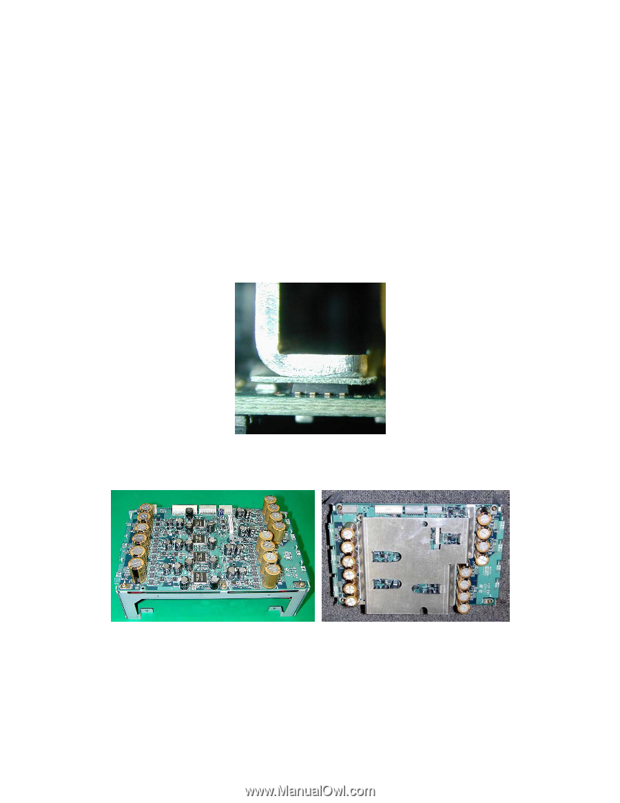
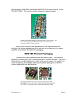
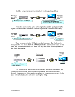
board, on which the transistors are surface mounted.
 |
View all Sony STR-DA2100ES manuals
Add to My Manuals
Save this manual to your list of manuals |
Page 13 highlights
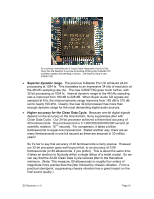
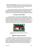
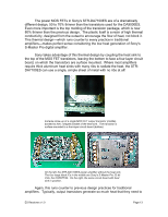
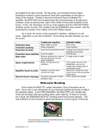
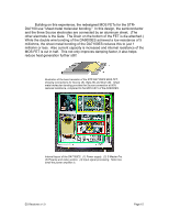
The power MOS FETs in Sony's STR-DA7100ES are of a dramatically different design, 50 to 70% thinner than the transistors used for the DA9000ES. Even more important is the top molding of the transistor package, which is now 80% thinner than the previous design. The plastic itself is a resin of high thermal conductivity, designed from the outset to encourage the flow of heat, not block it. This thermal design-which runs counter to every practice in traditional amplifiers-makes perfect sense considering the low heat generation of Sony's S-Master Pro digital amplifier. Sony takes advantage of this thermal design by coupling the heat sink to the top of the MOS FET transistors, leaving the bottom to face a four-layer circuit board, on which the transistors are surface mounted. Where most amplifiers require thick aluminum heat sinks with many ribs to radiate the heat, the STRDA7100ES can use a single, simple sheet of metal with no ribs at all! Extreme close-up of a single MOS FET output transistor (middle), bonded to the L-shaped bracket of the heat sink. The transistor is surface mounted to a four-layer circuit board (bottom). On the left, the STR-DA7100ES power amplifier without the heat sink. The four large black ICs in the middle are Sony's S-Master Pro 32-bit LSIs, the CXD9773Q. On the right, the same circuit board with heat sink in position. Again, this runs counter to previous design practices for traditional amplifiers. Typically, output transistors generate so much heat that they need to ES Receivers v1.0 Page 13
-
 1
1 -
2
-
3
-
4
-
5
-
6
-
7
-
 8
8 -
 9
9 -
 10
10 -
 11
11 -
 12
12 -
 13
13 -
 14
14 -
 15
15 -
 16
16 -
 17
17 -
 18
18 -
19
-
20
-
21
-
22
-
23
-
24
-
25
-
26
-
27
-
28
-
29
-
30
-
31
-
32
-
33
-
34
-
35
-
36
-
37
-
38
 |
 |