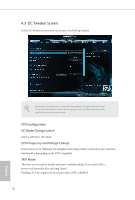
ASRock A320M-HDV R3.0 User Manual - Page 59
TwrwrDd, TrdrdSc, TrdrdSd, TrdrdDd, ProcODT, Data Bus Configuration, Gear Down Mode, Power Down
 |
View all ASRock A320M-HDV R3.0 manuals
Add to My Manuals
Save this manual to your list of manuals |
Page 59 highlights
TwrwrDd The minimum number of cycles from the last clock of virtual CAS of the first write-burst operation to the clock in which CAS is asserted for a following write-burst operation in a different DIMM. TrdrdSc The minimum number of cycles from the last clock of virtual CAS of the first read-burst operation to the clock in which CAS is asserted for a following read-burst operation in the same chipselect. TrdrdSd The minimum number of cycles from the last clock of virtual CAS of the first read-burst operation to the clock in which CAS is asserted for a following read-burst operation in the same DIMM. TrdrdDd The minimum number of cycles from the last clock of virtual CAS of the first read-burst operation to the clock in which CAS is asserted for a following read-burst operation in a different DIMM. tCKE Specifies the CKE minimum high and low pulse width in memory clock cycles. ProcODT Specifies the Processor ODT Data Bus Configuration Configure the RttNom, RttWr and RttPark. Gear Down Mode Power Down Enable CAD Bus Configuration Command Rate (CR) The delay between when a memory chip is selected and when the first active command can be issued. 54 English
-
 1
1 -
2
-
3
-
4
-
5
-
6
-
7
-
8
-
9
-
10
-
11
-
12
-
13
-
14
-
15
-
16
-
17
-
18
-
19
-
20
-
21
-
22
-
23
-
24
-
25
-
26
-
27
-
28
-
29
-
30
-
31
-
32
-
33
-
34
-
35
-
36
-
37
-
38
-
39
-
40
-
41
-
42
-
43
-
44
-
45
-
46
-
47
-
48
-
49
-
50
-
51
-
52
-
53
-
 54
54 -
 55
55 -
 56
56 -
 57
57 -
 58
58 -
 59
59 -
 60
60 -
 61
61 -
 62
62 -
 63
63 -
 64
64 -
65
-
66
-
67
-
68
-
69
-
70
-
71
-
72
-
73
-
74
-
75
-
76
-
77
-
78
-
79
-
80
-
81
-
82
-
83
-
84
-
85
-
86
-
87
 |
 |