ASRock B650E PG Riptide WiFi Software/BIOS Setup Guide - Page 35
Write to Read Delay tWTR_L, RAS to RAS Delay tRRD_L
 |
View all ASRock B650E PG Riptide WiFi manuals
Add to My Manuals
Save this manual to your list of manuals |
Page 35 highlights
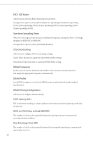
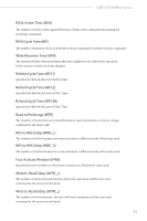
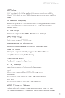
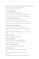
AMD X670/B650 Series RAS# Active Time (tRAS) The number of clock cycles required between a bank active command and issuing the precharge command. RAS# Cycle Time (tRC) The number of memory clock cycles from activate command to another activate command. Write Recovery Time (tWR) The amount of delay that must elapse after the completion of a valid write operation, before an active bank can be precharged. Refresh Cycle Time (tRFC1) Specifies the Refresh Recovery Delay Time. Refresh Cycle Time (tRFC2) Specifies the Refresh Recovery Delay Time. Refresh Cycle Time (tRFCSb) Specifies the Refresh Recovery Delay Time. Read to Precharge (tRTP) The number of clocks that are inserted between a read command to a row pre-charge command to the same rank. RAS to RAS Delay (tRRD_L) The number of clocks between two rows activated in different banks of the same rank. RAS to RAS Delay (tRRD_S) The number of clocks between two rows activated in different banks of the same rank. Four Activate Window (tFAW) Specifies the time window in which four activates are allowed the same rank. Write to Read Delay (tWTR_L) The number of clocks between the last valid write operation and the next read command to the same internal bank. Write to Read Delay (tWTR_L) The number of clocks between the last valid write operation and the next read command to the same internal bank. 31
-
 1
1 -
2
-
3
-
4
-
5
-
6
-
7
-
8
-
9
-
10
-
11
-
12
-
13
-
14
-
15
-
16
-
17
-
18
-
19
-
20
-
21
-
22
-
23
-
24
-
25
-
26
-
27
-
28
-
29
-
 30
30 -
 31
31 -
 32
32 -
 33
33 -
 34
34 -
 35
35 -
 36
36 -
 37
37 -
 38
38 -
 39
39 -
 40
40 -
41
-
42
-
43
-
44
-
45
-
46
-
47
-
48
-
49
-
50
-
51
-
52
-
53
-
54
-
55
-
56
-
57
-
58
-
59
-
60
-
61
-
62
-
63
-
64
-
65
-
66
-
67
-
68
-
69
-
70
-
71
-
72
-
73
-
74
-
75
-
76
-
77
-
78
-
79
-
80
-
81
-
82
-
83
-
84
-
85
 |
 |