ASRock J3455M User Manual - Page 22
Platform Module TPM system, Print Port Header
 |
View all ASRock J3455M manuals
Add to My Manuals
Save this manual to your list of manuals |
Page 22 highlights
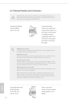
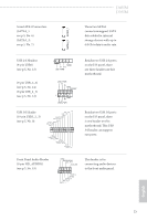
J3455M J3355M GN D +3VS B LAD0 +3V LAD3 PCIRST # FRAM E PCICLK TPM Header (17-pin TPMS1) (see p.5, No. 18) GND SERIRQ # S_PWRDWN # GN D LAD1 LAD2 SMB_DATA_MAIN SMB_CLK_MAIN GN D This connector supports Trusted Platform Module (TPM) system, 1 which can securely store keys, digital certificates, passwords, and data. A TPM system also helps enhance network security, protects digital identities, and ensures platform integrity. Print Port Header (25-pin LPT1) (see p.5, No. 15) STB# SPD0 SPD1 SPD2 SLCT PE BUSY SPD3 SPD4 SPD5 ACK# SPD6 SPD7 1 GND SLIN# PINIT# ERROR# AFD# This is an interface for print port cable that allows convenient connection of printer devices. BIOS_PH Connector (9-pin BIOS_PH) (see p.5, No. 1) SPI_DQ0 SPI_CLK SPI Power (1.8V) SPI_DQ3 GND SPI_DQ1 SPI_CS# SPI_DQ2 1 This header is for writing the BIOS into flash ROM when the BIOS ROM corrupts and the system cannot boot up. *This header is for factory engineering purpose. English 17
-
 1
1 -
2
-
3
-
4
-
5
-
6
-
7
-
8
-
9
-
10
-
11
-
12
-
13
-
14
-
15
-
16
-
 17
17 -
 18
18 -
 19
19 -
 20
20 -
 21
21 -
 22
22 -
 23
23 -
 24
24 -
 25
25 -
 26
26 -
 27
27 -
28
-
29
-
30
-
31
-
32
-
33
-
34
-
35
-
36
-
37
-
38
-
39
-
40
-
41
-
42
-
43
-
44
-
45
-
46
-
47
-
48
-
49
-
50
-
51
 |
 |
