ASRock K7S8X User Manual - Page 12
Connectors - cpu support
 |
View all ASRock K7S8X manuals
Add to My Manuals
Save this manual to your list of manuals |
Page 12 highlights
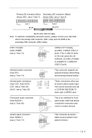
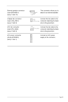
Note:The setting of the CPU front side bus frequency of this motherboard is by means of the adjustment of jumper-setting. Please follow the figures above to set the CPU front side bus frequency. Please note that the setting of FSB 200MHz will function only when the installed CPU supports FSB 200MHz. PS2_USB_PWR1 1_2 2_3 Short pin2, pin3 to enable (see p.7 item 22) +5V +5VSB +5VSB (standby) for PS/2 or USB wake up events. Note: To select +5VSB, it requires 2 Amp and higher standby current provided by power supply. CLRCMOS1 (see p.2 item 17) Clear CMOS CLRCMOS2 solder points (see p.2 item 27) 2-pin jumper Note: CLRCMOS1 and CLRCMOS2 allow you to clear the data in CMOS. The data in CMOS includes system setup information such as system password, date, time, and system setup parameters. There are 2 ways for you to clear and reset the system parameters to the default setup. Please turn off the computer and unplug the power cord, then you may either short the solder points on CLRCMOS1 by using metal material, e.g., a paper clip for 3 seconds; or you may use a jumper cap to short the pin on CLRCMOS2 for 3 seconds. Please remeber to remove the paper clip or the jumper cap after clearing the CMOS. 2.8 Connectors Connectors are NOT jumpers. DO NOT place jumper caps over these connectors. Connector Figure Description FDD connector (33-pin FLOPPY1) (see p.7 item 10) Pin1 FLOPPY1 Red marking Note: Match the red marking on the floppy ribbon cable with Pin1. 12
-
 1
1 -
2
-
3
-
4
-
5
-
6
-
 7
7 -
 8
8 -
 9
9 -
 10
10 -
 11
11 -
 12
12 -
 13
13 -
 14
14 -
 15
15 -
 16
16 -
 17
17 -
18
-
19
-
20
-
21
-
22
-
23
-
24
-
25
-
26
 |
 |