ASRock K7V88 User Manual - Page 15
Jumpers Setup
 |
View all ASRock K7V88 manuals
Add to My Manuals
Save this manual to your list of manuals |
Page 15 highlights
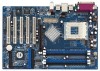
2.5 Jumpers Setup The illustration shows how jumpers are setup. When the jumper cap is placed on pins, the jumper is "Short". If no jumper cap is placed on pins, the jumper is "Open". The illustration shows a 3-pin jumper whose pin1 and pin2 are "Short" when jumper cap is placed on these 2 pins. Short Open Jumper Setting PS2_USB_PWR1 1_2 2_3 Short pin2, pin3 to enable (see p.8, No. 1) +5V +5VSB +5VSB (standby) for PS/2 or USB wake up events. Note: To select +5VSB, it requires 2 Amp and higher standby current provided by power supply. JR1(see p.8, No. 29) JL1(see p.8, No. 30) JR1 JL1 Note: If the jumpers JL1 and JR1 are short, both the front panel and the rear panel audio connectors can work. Clear CMOS (CLRCMOS2, 2-pin jumper) (see p.8, No. 23) 2-pin jumper Note: CLRCMOS2 allows you to clear the data in CMOS. The data in CMOS includes system setup information such as system password, date, time, and system setup parameters. To clear and reset the system parameters to default setup, please turn off the computer and unplug the power cord, then use a jumper cap to short the pins on CLRCMOS2 for 3 seconds. Please rem ember to remove the jumper cap after clearing the CMOS. If you need to clear the CMOS when you just finish updating the BIOS, you must boot up the system first, and then shut it down before you do the clear-CMOS action. FSB_SEL0 (see p.8, No. 9) FSB_SEL1 FSB_SEL0 FSB_SEL1 1_2 2_3 1_2 FSB_SEL0 1_2 FSB_SEL1 FSB_SEL0 FSB_SEL1 2_3 1_2 2_3 FSB_SEL0 2_3 FSB_SEL1 (see p.8, No. 10) FSB 200MHz FSB 266MHz FSB 333MHz FSB 400MHz Note: The setting of the CPU front side bus frequency of this motherboard is by means of the adjustment of jumper-setting. To perform over clocking, you must set the FSB jumper according to your AMD CPU before you use the "Manual" option as the FSB setting in BIOS setup. Please follow the figures above to set the CPU front side bus frequency. 15
-
 1
1 -
2
-
3
-
4
-
5
-
6
-
7
-
8
-
9
-
 10
10 -
 11
11 -
 12
12 -
 13
13 -
 14
14 -
 15
15 -
 16
16 -
 17
17 -
 18
18 -
 19
19 -
 20
20 -
21
-
22
-
23
-
24
-
25
-
26
-
27
-
28
-
29
-
30
-
31
-
32
-
33
-
34
-
35
-
36
-
37
 |
 |
