ASRock Z690 Taichi User Manual - Page 93
Initial RTL MC1 C1 B1/B2
 |
View all ASRock Z690 Taichi manuals
Add to My Manuals
Save this manual to your list of manuals |
Page 93 highlights
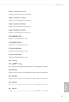
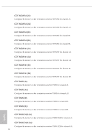
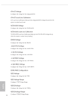
Initial RTL (MC0 C0 A1/A2) Configure round trip latency initial value. Initial RTL (MC0 C1 A1/A2) Configure round trip latency initial value. Initial RTL (MC1 C0 B1/B2) Configure round trip latency initial value. Initial RTL (MC1 C1 B1/B2) Configure round trip latency initial value. RTL (MC0 C0 A1/A2) Configure round trip latency value. RTL (MC0 C1 A1/A2) Configure round trip latency value. RTL (MC1 C0 B1/B2) Configure round trip latency value. RTL (MC1 C1 B1/B2) Configure round trip latency value. ODT Setting Dimm ODT Training ODT values will be optimized by Dimm On-Die Termination Training. ODT WR (A1) Configure the memory on die termination resistors' WR for channel A1. ODT WR (A2) Configure the memory on die termination resistors' WR for channel A2. ODT WR (B1) Configure the memory on die termination resistors' WR for channel B1. ODT WR (B2) Configure the memory on die termination resistors' WR for channel B2. Z690 Taichi 85 English
-
 1
1 -
2
-
3
-
4
-
5
-
6
-
7
-
8
-
9
-
10
-
11
-
12
-
13
-
14
-
15
-
16
-
17
-
18
-
19
-
20
-
21
-
22
-
23
-
24
-
25
-
26
-
27
-
28
-
29
-
30
-
31
-
32
-
33
-
34
-
35
-
36
-
37
-
38
-
39
-
40
-
41
-
42
-
43
-
44
-
45
-
46
-
47
-
48
-
49
-
50
-
51
-
52
-
53
-
54
-
55
-
56
-
57
-
58
-
59
-
60
-
61
-
62
-
63
-
64
-
65
-
66
-
67
-
68
-
69
-
70
-
71
-
72
-
73
-
74
-
75
-
76
-
77
-
78
-
79
-
80
-
81
-
82
-
83
-
84
-
85
-
86
-
87
-
 88
88 -
 89
89 -
 90
90 -
 91
91 -
 92
92 -
 93
93 -
 94
94 -
 95
95 -
 96
96 -
 97
97 -
 98
98 -
99
-
100
-
101
-
102
-
103
-
104
-
105
-
106
-
107
-
108
-
109
-
110
-
111
-
112
-
113
-
114
-
115
-
116
-
117
-
118
-
119
-
120
-
121
-
122
-
123
-
124
-
125
-
126
-
127
-
128
-
129
-
130
 |
 |