Asus D700-PV CUV4X User Manual - Page 60
Chip Configuration
 |
View all Asus D700-PV manuals
Add to My Manuals
Save this manual to your list of manuals |
Page 60 highlights
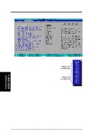
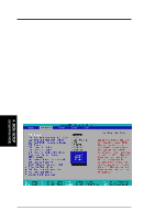
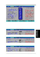
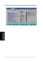
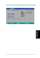
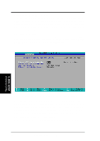
4. BIOS SETUP 4.4.1 Chip Configuration 4. BIOS SETUP Chip Configuration (Scroll down to see more items as shown here.) SDRAM Configuration [By SPD] This sets the optimal timings for items 2-5, depending on the memory modules that you are using. Default setting is [By SPD], which configures items 2-5 by reading the contents in the SPD (Serial Presence Detect) device. The EEPROM on the memory module stores critical parameter information about the module, such as memory type, size, speed, voltage interface, and module banks. Configuration options: [User Define] [7ns (143MHz)] [8ns (125MHz)] [By SPD] SDRAM CAS Latency This controls the latency between the SDRAM read command and the time that the data actually becomes available. NOTE: This field will only be displayed when SDRAM Configuration is set to [User Define]. SDRAM RAS Precharge Time This controls the idle clocks after issuing a precharge command to the SDRAM. NOTE: This field will only be displayed when SDRAM Configuration is set to [User Define]. SDRAM RAS to CAS Delay This controls the latency between the SDRAM active command and the read/write command. NOTE: This field will only be displayed when SDRAM Configuration is set to [User Define]. SDRAM Active to Precharge Time To make changes to this field, the SDRAM Configuration field must be set to [User Define]. 60 ASUS CUV4X User's Manual
-
 1
1 -
2
-
3
-
4
-
5
-
6
-
7
-
8
-
9
-
10
-
11
-
12
-
13
-
14
-
15
-
16
-
17
-
18
-
19
-
20
-
21
-
22
-
23
-
24
-
25
-
26
-
27
-
28
-
29
-
30
-
31
-
32
-
33
-
34
-
35
-
36
-
37
-
38
-
39
-
40
-
41
-
42
-
43
-
44
-
45
-
46
-
47
-
48
-
49
-
50
-
51
-
52
-
53
-
54
-
 55
55 -
 56
56 -
 57
57 -
 58
58 -
 59
59 -
 60
60 -
 61
61 -
 62
62 -
 63
63 -
 64
64 -
 65
65 -
66
-
67
-
68
-
69
-
70
-
71
-
72
-
73
-
74
-
75
-
76
-
77
-
78
-
79
-
80
-
81
-
82
-
83
-
84
-
85
-
86
-
87
-
88
-
89
-
90
-
91
-
92
-
93
-
94
-
95
-
96
-
97
-
98
-
99
-
100
-
101
-
102
-
103
-
104
 |
 |
