Asus P4G800-V P4G800-V user's manual English version E1352B - Page 46
Chipset
 |
View all Asus P4G800-V manuals
Add to My Manuals
Save this manual to your list of manuals |
Page 46 highlights
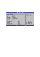
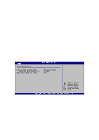
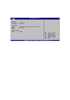
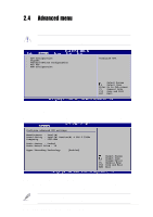
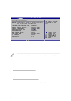
2.4.2 Chipset The Chipset menu items allow you to change the advanced chipset settings. Select an item then press Enter to display the sub-menu. Advanced Chipset settings WARNING: Setting wrong values in the sections below may cause system to malfunction. Configure DRAM Timing by SPD [Enabled] Graphic Adapter Priority Onboard Video Memory Graphics Aperture Size Spread Spectrum [AGP/Int. VGA] [Enabled, 8MB] [ 64 MB] [Enabled] Boot Display Device Flat Panel Type TV Standard [Auto] [640x480 LVDS] [Auto] MPS Revision [1.4] Set the CPU external frequency for next boot. Select Screen Select Item +- Change Option F1 General Help F10 Save and Exit ESC Exit Configure DRAM Timing by SPD [Enabled] When this item is enabled, the DRAM timing parameters are set according to the DRAM SPD (Serial Presence Detect). When disabled, you can manually set the DRAM timing parameters through the DRAM sub-items. Configuration options: [Disabled] [Enabled] The following sub-items appear when the item Configure DRAM Timing by SPD is set to Disabled. DRAM CAS# Latency [2.5 Clocks] This item controls the latency between the SDRAM read command and the time the data actually becomes available. Configuration options: [2.0 Clocks] [2.5 Clocks] [3.0 Clocks] DRAM RAS# Precharge [4 Clocks] This item controls the idle clocks after issuing a precharge command to the DDR SDRAM. Configuration options: [4 Clocks] [3 Clocks] [2 Clocks] DRAM RAS# to CAS# Delay [4 Clocks] This item controls the latency between the DDR SDRAM active command and the read/write command. Configuration options: [4 Clocks] [3 Clocks] [2 Clocks] 2-14 Chapter 2: BIOS information
-
 1
1 -
2
-
3
-
4
-
5
-
6
-
7
-
8
-
9
-
10
-
11
-
12
-
13
-
14
-
15
-
16
-
17
-
18
-
19
-
20
-
21
-
22
-
23
-
24
-
25
-
26
-
27
-
28
-
29
-
30
-
31
-
32
-
33
-
34
-
35
-
36
-
37
-
38
-
39
-
40
-
 41
41 -
 42
42 -
 43
43 -
 44
44 -
 45
45 -
 46
46 -
 47
47 -
 48
48 -
 49
49 -
 50
50 -
 51
51 -
52
-
53
-
54
-
55
-
56
-
57
-
58
-
59
-
60
-
61
-
62
-
63
-
64
-
65
-
66
-
67
-
68
 |
 |
