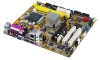
Asus P5VD2 MX Motherboard Installation Guide - Page 71
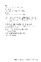
CAS Latency Time [2.5], Bank Interleave [Disabled], Precharge to Active Trp [4T] - vga
 |
UPC - 610839154326
View all Asus P5VD2 MX manuals
Add to My Manuals
Save this manual to your list of manuals |
Page 71 highlights
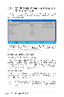
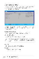
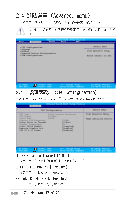
Advanced Phoenix-Award BIOS Setup Utility Chipset Select Menu DARM Clock/Drive Control Frequency/Voltage control Top Performance Primary Display Adapter VGA Share Memory Size [Disabled] [PCI-E] [64M] Item Specific Help Advanced Phoenix-Award BIOS Setup Utility DRAM Clock/Drive Control Select Menu Current DRAM Frequency DRAM Frequency DRAM Timing Selectable x CAS Lateency x Bank Interleave x Precharge to Active(Trp) x Active to CMD(Trcd) x REF to ACT/REF(Trfc) x ACT(0) to ACT(1) (TRBD) 200MHz Auto [By SPD] 2.5 Disabled 4T 07T 20T/21T 3T Item Specific Help CAS Latency Time [2.5] Bank Interleave [Disabled] Precharge to Active (Trp) [4T] 2-21
-
 1
1 -
2
-
3
-
4
-
5
-
6
-
7
-
8
-
9
-
10
-
11
-
12
-
13
-
14
-
15
-
16
-
17
-
18
-
19
-
20
-
21
-
22
-
23
-
24
-
25
-
26
-
27
-
28
-
29
-
30
-
31
-
32
-
33
-
34
-
35
-
36
-
37
-
38
-
39
-
40
-
41
-
42
-
43
-
44
-
45
-
46
-
47
-
48
-
49
-
50
-
51
-
52
-
53
-
54
-
55
-
56
-
57
-
58
-
59
-
60
-
61
-
62
-
63
-
64
-
65
-
 66
66 -
 67
67 -
 68
68 -
 69
69 -
 70
70 -
 71
71 -
 72
72 -
 73
73 -
 74
74 -
 75
75 -
 76
76 -
77
-
78
-
79
-
80
-
81
-
82
-
83
-
84
-
85
-
86
-
87
-
88
-
89
-
90
-
91
-
92
-
93
-
94
-
95
-
96
-
97
-
98
-
99
-
100
-
101
-
102
-
103
-
104
-
105
-
106
-
107
-
108
-
109
-
110
-
111
-
112
 |
 |
2-21
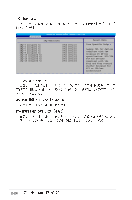
Chipset
DARM Clock/Drive Control
Frequency/Voltage control
Top Performance
[Disabled]
Primary Display Adapter
[PCI-E]
VGA Share Memory Size
[64M]
Select Menu
Item Specific Help
Phoenix-Award BIOS Setup Utility
Advanced
DRAM Clock/Drive Control
Current DRAM Frequency
200MHz
DRAM Frequency
Auto
DRAM Timing Selectable
[By SPD]
x CAS Lateency
2.5
x Bank Interleave
Disabled
x Precharge to Active(Trp)
4T
x Active to CMD(Trcd)
07T
x REF to ACT/REF(Trfc)
20T/21T
x ACT(0) to ACT(1) (TRBD)
3T
Select Menu
Item Specific Help
Phoenix-Award BIOS Setup Utility
Advanced
CAS Latency Time [2.5]
Bank Interleave [Disabled]
Precharge to Active (Trp) [4T]