Biostar U8668 U8668 BIOS setup guide - Page 13
AGP & P2P Bridge Control
 |
View all Biostar U8668 manuals
Add to My Manuals
Save this manual to your list of manuals |
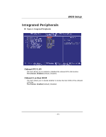
Page 13 highlights
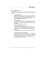
BIOS Setup DRAM Timing This item determines DRAM clock/ timing follow SPD or not. The Choices: By SPD(default), Manual. SDRAM CAS Latency When DRAM is installed, the number of clock cycles of CAS latency depends on the DRAM timing. The Choices: 2.5 (default), 2. Bank Interleave This item allows you to enable or disable the bank interleave feature. The Choices: Disabled (default). Precharge to Active (Trp) This items allows you to specify the delay from precharge command to activate command. The Choices: 2T, 3T (default). Active to Precharge (Tras) This items allows you to specify the minimum bank active time. The Choices: 6T (default), 5T. Active to CMD (Trcd) Use this item to specify the delay from the activation of a bank to the time that a read or write command is accepted. The Choices: 2T, 3T (default). DRAM Burst Len The Choices: 4 (default), 8. DRAM Command Rate This item controls clock cycle that must occur between the last valid write operation and the next command. The Choices: 1T Command, 2T Command (default). AGP & P2P Bridge Control If you highlight the literal "Press Enter" next to the "AGP & P2P Bridge Control" label and then press the enter key, it will take you a submenu with the following options: AGP Aperture Size Select the size of the Accelerated Graphics Port (AGP) aperture. The aperture is a portion of the PCI memory address range dedicated for graphics memory address space. Host cycles that hit the aperture range are forwarded to the AGP without any translation. The Choices: 64M (default), 256M, 128M, 32M, 16M, 8M, 4M. - 12 -
-
 1
1 -
2
-
3
-
4
-
5
-
6
-
7
-
 8
8 -
 9
9 -
 10
10 -
 11
11 -
 12
12 -
 13
13 -
 14
14 -
 15
15 -
 16
16 -
 17
17 -
 18
18 -
19
-
20
-
21
-
22
-
23
-
24
-
25
-
26
-
27
-
28
-
29
-
30
-
31
-
32
-
33
-
34
-
35
 |
 |
