Compaq ProLiant 400 Memory technology evolution: an overview of system memory - Page 5
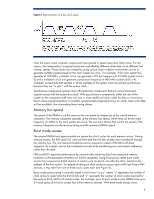
Memory bus speed, Burst mode access, sequence. As a result
 |
View all Compaq ProLiant 400 manuals
Add to My Manuals
Save this manual to your list of manuals |
Page 5 highlights
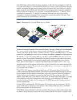
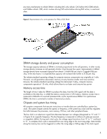
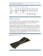
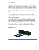
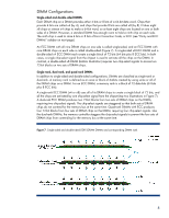
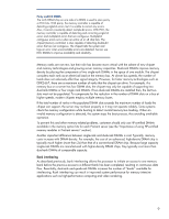
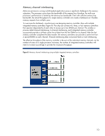
Figure 3. Representation of a bus clock signal Over the years, some computer components have gained in speed more than others have. For this reason, the components in a typical server are controlled by different clocks that run at different, but related, speeds. These clocks are created by using various clock multiplier and divider circuits to generate multiple signals based on the main system bus clock. For example, if the main system bus operates at 100 MHz, a divider circuit can generate a PCI bus frequency of 33 MHz (system clock ÷ 3) and a multiplier circuit can generate a processor frequency of 400 MHz (system clock x 4). Computer components that operate in whole multiples of the system clock are termed synchronous because they are "in sync" with the system clock. Synchronous components operate more efficiently than components that are not synchronized (asynchronous) with the system bus clock. With asynchronous components, either the rest of the system or the component itself must wait one or more additional clock cycles for data or instructions due to clock resynchronization. In contrast, synchronized components know on which clock cycle data will be available, thus eliminating these timing delays. Memory bus speed The speed of the DRAM is not the same as the true speed (or frequency) of the overall memory subsystem. The memory subsystem operates at the memory bus speed, which may not be the same frequency (in MHz) as the main system bus clock. The two main factors that control the speed of the memory subsystem are the memory timing and the maximum DRAM speed. Burst mode access The original DRAM took approximately six system bus clock cycles for each memory access. During memory access, the RAS and CAS were sent first and then 64 bits of data were transferred through the memory bus. The next sequential address access required a repeat of the RAS-CAS-Data sequence. As a result, most of the overhead occurred while transferring row and column addresses, rather than the data. FPM and EDO improved performance by automatically retrieving data from sequential memory locations on the assumption that they too will be requested. Using this process called burst mode access, four consecutive 64-bit sections of memory are accessed, one after the other, based on the address of the first section. So instead of taking six clock cycles to access each of the last three 64-bit sections, it may take from one to three clock cycles each (see Figure 4). Burst mode access timing is normally stated in the format "x-y-y-y" where "x" represents the number of clock cycles to read/write the first 64 bits and "y" represents the number of clock cycles required for the second, third, and fourth reads/writes. For example, prior to burst mode access, DRAM took up to 24 clock cycles (6-6-6-6) to access four 64-bit memory sections. With burst mode access, three 5
-
 1
1 -
 2
2 -
 3
3 -
 4
4 -
 5
5 -
 6
6 -
 7
7 -
 8
8 -
 9
9 -
 10
10 -
 11
11 -
12
-
13
-
14
-
15
-
16
-
17
-
18
-
19
-
20
 |
 |
