Foxconn H61MXV User manual - Page 36
Memory Timing Configuration
 |
View all Foxconn H61MXV manuals
Add to My Manuals
Save this manual to your list of manuals |
Page 36 highlights
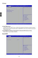
Memory Timing Configuration Aptio Setup Utility - C opyright (C) 2012 American Megatrends, Inc. F-Center Memory Multiplier Configuration Performance Memory Profiles XMP Profile 1 XMP Profile 2 [Manual] Not Supported Not Supported The selection of Performance Memory Profiles which impacts memory sizing behavior. Memory Timing Configuration Memory Clock Multiplier Memory Multiplirer tCL tRP tRCD tRAS tWR tRFC tWTR tRRD tRTP tFAW Intel Graphics Configuration [1.33] [13.33] 9 9 9 24 10 74 5 4 5 20 → ←: Select Screen ↑ ↓: Select Item Enter: Select +/-: Change Opt. F1: General Help F2: Previous Values F3: Optimized Defaults F4: Save & Reset ESC: Exit Graphics Core Ratio Limit 22 Version 2.14.1219. Copyright (C) 2012 American Megatrends, Inc. 3 ► CAS Latency (tCL) The number of memory clocks it takes a DRAM to return data after the read CAS_L is assert ed depends on the memory clock frequency. The value that BIOS programs into the memory controller is a function of the target clock frequency. The target clock frequency is determined from the supported CAS latencies at given clock frequencies of each DIMM. ► Row Precharge Time (tRPmin) This item allows you to select the row precharge time (in clock cycles). ► CAS to RAS(tRCDmin) This item allows you to select a delay time (in clock cycles) between the CAS# and RAS# strobe signals. ► Active to Precharge(tRASmin) This item allows you to set the minimum RAS# active time (in clock cycles). ► Write Recovery(tWRmin) This item allows you to select the write recovery time (in clock cycles). ► Refresh Recovery(tRFCmin) Refresh to Refresh or Refresh to Active command interval. ► Internal Write to Read Command(tWTR) This item allows you to select a delay time (in clock cycles) between sending the last data from a write operation to the memory and issuing a read command. ► Row Active to Row Active(tRRDmin) This item allows you to select a delay time (in clock cycles) between the RAS# and RAS# strobe signals. ► Read CAS# Precharge Delay (tRTP) 29
-
 1
1 -
2
-
3
-
4
-
5
-
6
-
7
-
8
-
9
-
10
-
11
-
12
-
13
-
14
-
15
-
16
-
17
-
18
-
19
-
20
-
21
-
22
-
23
-
24
-
25
-
26
-
27
-
28
-
29
-
30
-
 31
31 -
 32
32 -
 33
33 -
 34
34 -
 35
35 -
 36
36 -
 37
37 -
 38
38 -
 39
39 -
 40
40 -
 41
41 -
42
-
43
-
44
-
45
-
46
-
47
-
48
-
49
-
50
-
51
-
52
-
53
-
54
-
55
-
56
-
57
-
58
-
59
-
60
-
61
-
62
-
63
-
64
-
65
-
66
-
67
-
68
-
69
-
70
-
71
-
72
-
73
 |
 |
