Foxconn P55A-S English Manual. - Page 33
Fox Central Control Unit
 |
View all Foxconn P55A-S manuals
Add to My Manuals
Save this manual to your list of manuals |
Page 33 highlights
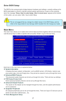
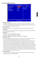
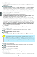
► PCI IDE BusMaster This item is used to enable/disable PCI IDE busmaster function, BIOS use PCI busmastering for read/write to IDE drives. Fox Central Control Unit CMOS Setup Utility - Copyright (C) 1985-2009, American Megatrends, Inc. FOX Central Control Unit ► CPU Configuration [Press Enter] Help Item ► Voltage Options [Press Enter] ******* Ratio and Clock Setting ****** Configure CPU. Ratio Status:Unlocked (Min:09, Max:22) Ratio Actual Value:22 CPU Clock Ratio [22] ******* Memory Frequency ****** Current DRAM Speed :800MHz DRAM Frequency [Auto] Memory Timing by SPD [Auto] BIOS Write Protect [Enabled] 3 Move Enter:Select +/-/:Value F10:Save ESC:Exit F1:General Help F9:Optimized Defaults ► CPU Configuration / Voltage Options Press to go to its submenu. ► CPU Clock Ratio This item is used to set the ratio between CPU Core Clock and the FSB Frequency. You can use [+] or [-] to adjust the value. ► DRAM Frequency This item is used to set DRAM frequency. Setting values are: [Auto], [800 MHz], [1067 MHz], [1333 MHz]. ► Memory Timing by SPD This item is used to enable/disable provision of DRAM timing by SPD device. The Serial Presence Detect (SPD) device is a small EEPROM chip, mounted on a memory module. It contains important information about the module's speed, size, addressing mode and various other parameters, so that the motherboard memory controller (chipset) can better access the memory device. Select [Auto] for SPD enable mode. Select [Manual] to set the parameters by yourself. The following 10 settings are valid only when Memory Timing by SPD is set to [Manual]. ► DRAM tCL The number of memory clocks it takes a DRAM to return data after the read CAS_L is asserted depends on the memory clock frequency. The value that BIOS programs into the memory controller is a function of the target clock frequency. The target clock frequency is determined from the supported CAS latencies at given clock frequencies of each DIMM. ► DRAM tRAS (Active-to-Precharge Delay) This item allows you to set the minimum RAS# active time (in clock cycles). ► DRAM tRP (Precharge Command Period) 26
-
 1
1 -
2
-
3
-
4
-
5
-
6
-
7
-
8
-
9
-
10
-
11
-
12
-
13
-
14
-
15
-
16
-
17
-
18
-
19
-
20
-
21
-
22
-
23
-
24
-
25
-
26
-
27
-
 28
28 -
 29
29 -
 30
30 -
 31
31 -
 32
32 -
 33
33 -
 34
34 -
 35
35 -
 36
36 -
 37
37 -
 38
38 -
39
-
40
-
41
-
42
-
43
-
44
-
45
-
46
-
47
-
48
-
49
-
50
-
51
-
52
-
53
-
54
-
55
-
56
-
57
-
58
-
59
-
60
-
61
-
62
-
63
-
64
-
65
-
66
-
67
-
68
-
69
-
70
-
71
-
72
-
73
-
74
-
75
-
76
-
77
-
78
-
79
-
80
-
81
-
82
-
83
-
84
-
85
-
86
-
87
-
88
-
89
-
90
-
91
-
92
-
93
-
94
-
95
-
96
-
97
-
98
-
99
-
100
-
101
-
102
-
103
-
104
-
105
-
106
-
107
-
108
-
109
-
110
-
111
-
112
-
113
-
114
 |
 |
