HP BL40p Memory technology evolution: an overview of system memory technologie - Page 4
DRAM storage density and power consumption
 |
UPC - 613326517680
View all HP BL40p manuals
Add to My Manuals
Save this manual to your list of manuals |
Page 4 highlights
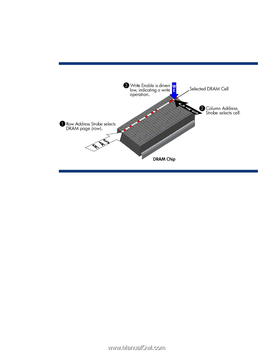
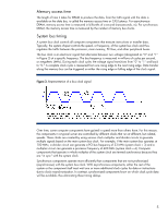
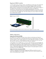
When FPM or EDO memory writes data to a particular cell, the memory controller selects the location in which to write the data. The memory controller first selects the page by strobing the Row Address onto the address/command bus. It then selects the exact location by strobing the Column Address onto the address/command bus (see Figure 2). These actions are called Row Address Strobe (RAS) and Column Address Strobe (CAS). The Write Enable (WE) signal is activated at the same time as the CAS to specify that a write operation is to be performed. The memory controller then drives the data onto the memory bus. The DRAM devices capture (latch) the data and store it into the respective cells. Figure 2. Representation of a write operation for FPM or EDO RAM During a DRAM read operation, RAS followed by CAS are driven onto the memory bus. The WE signal is held inactive, indicating a read operation. After a delay called CAS Latency, the DRAM devices drive the data onto the memory bus. DRAM cannot be accessed during a refresh. If the processor makes a data request during a DRAM refresh, the data will not be available until the refresh completes. There are many mechanisms to refresh DRAM, including RAS only refresh, CAS before RAS (CBR) refresh, and Hidden refresh. CBR, which involves driving CAS active before driving RAS active, is used most often. DRAM storage density and power consumption The storage capacity (density) of DRAM is inversely proportional to the cell geometry. In other words, storage density increases as cell geometry shrinks. Over the past few years, improvements in DRAM storage density have increased capacity from almost 1 kilobit (Kb) per chip to 2 gigabit (Gb) per chip. In the near future, it is expected that capacity will increase even further to 4 Gb per chip. The industry-standard operating voltage for computer memory components was originally 5 volts. However, as cell geometries decreased, memory circuitry became smaller and more sensitive. Likewise, the industry-standard operating voltage decreased. Today, computer memory components operate at 1.8 volts, which allows them to run faster and consume less power. 4
-
 1
1 -
 2
2 -
 3
3 -
 4
4 -
 5
5 -
 6
6 -
 7
7 -
 8
8 -
 9
9 -
 10
10 -
11
-
12
-
13
-
14
-
15
-
16
-
17
-
18
-
19
-
20
-
21
-
22
-
23
-
24
 |
 |