HP C4137A Memory technology evolution: an overview of system memory technologi - Page 6
Memory bus speed, Burst mode access
 |
UPC - 088698192719
View all HP C4137A manuals
Add to My Manuals
Save this manual to your list of manuals |
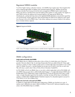
Page 6 highlights
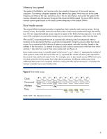
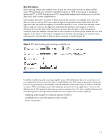
Memory bus speed The speed of the DRAM is not the same as the true speed (or frequency) of the overall memory subsystem. The memory subsystem operates at the memory bus speed, which may not be the same frequency (in MHz) as the main system bus clock. The two main factors that control the speed of the memory subsystem are the memory timing and the maximum DRAM speed. The server BIOS sets the memory system speed based on the fastest common frequency of the loaded DIMMs. Burst mode access The original DRAM took approximately six system-bus clock cycles for each memory access. During memory access, first the RAS and CAS and then 64 bits of data were transferred through the memory bus. The next sequential address access required a repeat of the RAS-CAS-Data sequence. As a result, most of the overhead occurred while transferring row and column addresses, rather than the data. FPM and EDO improved performance by automatically retrieving data from sequential memory locations on the assumption that they would also be requested. Using this process called burst mode access, four consecutive 64-bit sections of memory are accessed, one after the other, based on the address of the first section. So instead of taking six clock cycles to access each of the last three 64-bit sections, it may take from one to three clock cycles each (see Figure 4). Burst mode access timing is normally stated in the format "x-y-y-y" where "x" represents the number of clock cycles to read/write the first 64 bits and "y" represents the number of clock cycles required for the second, third, and fourth reads/writes. For example, prior to burst mode access, DRAM took up to 24 clock cycles (6-6-6-6) to access four 64-bit memory sections. With burst mode access, three additional data sections are accessed with every clock cycle after the first access (6-1-1-1) before the memory controller has to send another CAS. Figure 4. Burst mode access Clock Command Address Data Active NOP NOP Read NOP NOP NOP NOP NOP NOP Row Col Data Data Data Data 64b 64b 64b 64b NOTE: NOP = No Operation Instruction 6
-
 1
1 -
 2
2 -
 3
3 -
 4
4 -
 5
5 -
 6
6 -
 7
7 -
 8
8 -
 9
9 -
 10
10 -
 11
11 -
 12
12 -
13
-
14
-
15
-
16
-
17
-
18
-
19
-
20
-
21
-
22
-
23
-
24
 |
 |