HP ProLiant SL160s Memory technology evolution: an overview of system memory t - Page 5
Memory bus speed, Burst mode access, SDRAM technology
 |
View all HP ProLiant SL160s manuals
Add to My Manuals
Save this manual to your list of manuals |
Page 5 highlights
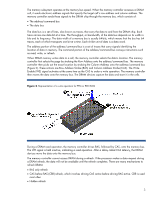
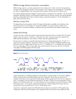
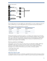
cycles for data or instructions. In contrast, synchronized components know which clock cycle will make data available, eliminating these timing delays. Memory bus speed DRAM speed is not the same as the true speed, or frequency, of the memory subsystem. The memory subsystem operates at the memory bus speed, which may not be the same frequency (in MHz) as the main system bus clock. Memory timing and maximum DRAM speed control memory subsystem speed. The server BIOS sets the memory system speed based on the fastest common frequency of the loaded DIMMs. Burst mode access The original DRAM took about six system-bus clock cycles for each memory access. During memory access, first the RAS, CAS, and then 64 bits of data moved through the memory bus. The next sequential address access required a repeat of the RAS-CAS-Data sequence. As a result, most of the overhead occurred while transferring row and column addresses, not data. Later DRAM implementations improved performance by retrieving data from sequential memory locations on the assumption that the system will use all of the data. Called burst mode access, this process accesses four consecutive 64-bit sections of memory, one after the other, based on the address of the first section. So instead of taking six clock cycles to access each of the last three 64-bit sections, it can take from one to three clock cycles each (see Figure 4). Burst mode access timing is normally stated in the format "x-y-y-y" where "x" represents the number of clock cycles to read/write the first 64 bits and "y" represents the number of clock cycles required for the second, third, and fourth reads/writes. For example, prior to burst mode access, DRAM took up to 24 clock cycles (6-6-6-6) to access four 64-bit memory sections. With burst mode access, DRAM accesses three additional data sections with every clock cycle after the first access (6-1-1-1) before the memory controller has to send another CAS. Figure 4. Burst mode access Clock Command Address Data Active NOP NOP Read NOP NOP NOP NOP NOP NOP Row Col Data Data Data Data 64b 64b 64b 64b NOTE: NOP = No Operation Instruction SDRAM technology DRAMs are asynchronous, that is, without a memory bus clock. The memory controller determines when to assert signals and when to expect data based on absolute timing. Transferring data between a synchronous system bus and an asynchronous memory bus is inefficient and results in longer latency. Consequently, the JEDEC developed the synchronous DRAM standard to reduce the number of system clock cycles required to read or write data. SDRAM uses a memory bus clock to synchronize the input and output signals on the memory chip. This simplifies the memory controller and reduces CPU-to-memory latency. In 5
-
 1
1 -
 2
2 -
 3
3 -
 4
4 -
 5
5 -
 6
6 -
 7
7 -
 8
8 -
 9
9 -
 10
10 -
 11
11 -
12
-
13
-
14
-
15
-
16
-
17
-
18
-
19
 |
 |
