HP ProLiant SL390s Memory technology evolution: an overview of system memory t - Page 6
Bank interleaving, Increased bandwidth, Registered SDRAM modules, DIMM configurations
 |
View all HP ProLiant SL390s manuals
Add to My Manuals
Save this manual to your list of manuals |
Page 6 highlights
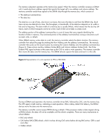
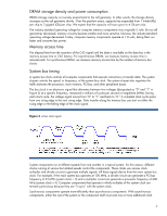
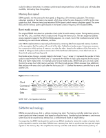
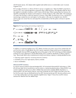
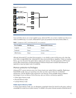
addition to synchronous operation and burst mode access, SDRAM has other features that accelerate data retrieval and increase memory capacity: • Multiple memory banks • Greater bandwidth • Register logic chips. Bank interleaving SDRAM divides memory into two to four banks for simultaneous access to more data. This division and simultaneous access is interleaving. Two-way interleaving is similar to dividing each page in a notebook into two parts and having two assistants retrieve a different part of the page. Even though each assistant must take a break, breaks are staggered so that at least one assistant is working at all times. Both assistants retrieve the data much faster than a single assistant does, especially since the single assistant does not access data when taking a break. This means that while the processor accesses one memory bank, the other bank stands ready for access. The processor can initiate a new memory access before the previous access completes, which results in continuous data flow. Increased bandwidth Memory bus bandwidth increases with its width (in bits) and its frequency (in MHz). By transferring 8 bytes (64 bits) at a time and running at 100 MHz, SDRAM increases memory bandwidth to 800 MB/s, 50% more than EDO DRAMs (533 MB/s at 66 MHz). Registered SDRAM modules To increase memory subsystem capacity, designers can embed register logic chips, referred to as registers, in DIMMs to act as pass-through buffers for address and command signals. With these registers, the memory controller does not have to drive the entire arrangement of DRAM chips on each module. Rather, the memory controller loads only the registers on each module. Each DIMM's register relays the address and command signals to the appropriate DRAM chip. Simultaneously, a phase-locked loop chip on a registered DIMM generates a second clock signal that runs synchronously with the system bus clock. This means the system bus clock does not have to drive all the DRAM chips. This lets you add more memory modules to the memory bus, increasing capacity. DIMM configurations DIMMs are available in several configurations, depending on the number and type of DRAMs used as well as the number of memory blocks, called ranks, the DIMM supports. Single-sided and double-sided DIMMs Each DRAM chip on a DIMM provides either 4 bits or 8 bits of a 64-bit data word. Chips that provide 4 bits are called x4 (by 4), and chips that provide 8 bits are called x8. Eight x8 chips or sixteen x4 chips make a 64-bit word, so at least eight chips are located on one or both sides of a DIMM. However, a standard DIMM has enough room to hold a ninth chip on each side. The ninth chip stores 4 bits or 8 bits of Error Correction Code (ECC). An ECC DIMM with nine DRAM chips on one side is single-sided, and an ECC DIMM with nine DRAM chips on each side is double-sided (Figure 5). A single-sided x8 ECC DIMM and a double-sided x4 ECC DIMM each create a single block of 72 bits (64 bits plus 8 ECC bits). In both cases, a single chip-select signal from the memory controller activates all the chips on the DIMM. In contrast, a double-sided x8 DIMM (bottom illustration) requires two chip-select signals to access two 72-bit blocks on two sets of DRAM chips. 6
-
 1
1 -
 2
2 -
 3
3 -
 4
4 -
 5
5 -
 6
6 -
 7
7 -
 8
8 -
 9
9 -
 10
10 -
 11
11 -
 12
12 -
13
-
14
-
15
-
16
-
17
-
18
-
19
 |
 |
