HP Rx2620-2 Installation Guide, Third Edition - HP Integrity rx2620 (August 20 - Page 22
Memory Block Diagram, Memory, Controller, DIMM1B
 |
UPC - 829160435749
View all HP Rx2620-2 manuals
Add to My Manuals
Save this manual to your list of manuals |
Page 22 highlights
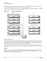
Introduction System Board Components The minimum amount of memory supported by the server is 1 GB (four 256 MB modules). The maximum amount of memory supported by the server is 32 GB (eight 4 GB modules). This design does not support any non industry standard DDR DIMMs. Only qualified DIMMs are supported. Figure 1-5 shows a block diagram of the server memory. Figure 1-5 Memory Block Diagram MC0 Parallel Termination Resistors for Address and Control Rt=27 ohms Parallel Termination Resistors for DQ[143:72] and associated DQS Rt=27 ohms SA0=1 SA1=0 SA2=0 DIMM0B CS1(0) CS1(4) SA0=1 SA1=0 SA2=1 DIMM CLK Stub Isolation Resistors Rs=0 ohms DIMM4B CS1(2) CS1(6) SA0=1 SA1=0 SA2=0 SA0=1 SA1=0 SA2=1 MC1 DIMM1B CS1(0) CS1(4) DIMM5B CS1(2) CS1(6) SA0=1 SA1=1 SA2=0 DIMM2B CS1(1) CS1(5) Stub Isolation Resistors for DQ[143:72] and associated DQS Rs=18 ohms DIMM CLK Stub Isolation Resistors Rs=0 ohms Parallel Termination Resistors for DQ [71:0] and associated DQS Rt=27 ohms SA0=0 SA1=0 SA2=0 DIMM0A CS1(0) CS1(4) SA0=1 SA1=1 SA2=0 DIMM3B CS1(1) CS1(5) Same connection scheme for MC1 as for MC0 SA0=0 SA1=0 SA2=0 DIMM1A CS1(0) CS1(4) SA0=0 SA1=0 SA2=1 DIMM4A CS1(2) CS1(6) SA0=0 SA1=1 SA2=0 DIMM CLK Stub Isolation Resistors Rs=0 ohms DIMM2A CS1(1) CS1(5) Stub Isolation Resistors for DQ[71:0] and associated DQS Rs=18 ohms Stub Isolation Resistors for Address and Control Rs=18 ohms Memory Controller SA0=0 SA1=0 SA2=1 SA0=0 SA1=1 SA2=0 DIMM5A DIMM3A CS1(2) CS1(6) CS1(1) CS1(5) Memory Architecture The I/O ASIC memory interface supports two DDR cells, each of which is 144 data bits wide. The memory subsystem physical design uses a comb-filter termination scheme for both the data and the address and control buses. This part of the topology is similar to other DDR designs in the computer industry. Clocks are distributed directly from the I/O ASIC; each clock pair drives 2 DIMMs. Memory data is protected by the ECC. Eight ECC bits per DIMM protect 64 bits of data. The use of ECC allows correction of single-bit errors, and detection of multi-bit errors. Only DIMMs with ECC are qualified or supported. DIMMs The memory subsystem supports only DDR SDRAM (Double Data Rate Synchronous Dynamic Random Access Memory) technology utilizing industry-standard PC-1600 type DDR SDRAM DIMMs, 1.2" tall. The DIMMs use a 184-pin JEDEC standard connector. 22 Chapter 1
-
 1
1 -
2
-
3
-
4
-
5
-
6
-
7
-
8
-
9
-
10
-
11
-
12
-
13
-
14
-
15
-
16
-
 17
17 -
 18
18 -
 19
19 -
 20
20 -
 21
21 -
 22
22 -
 23
23 -
 24
24 -
 25
25 -
 26
26 -
 27
27 -
28
-
29
-
30
-
31
-
32
-
33
-
34
-
35
-
36
-
37
-
38
-
39
-
40
-
41
-
42
-
43
-
44
-
45
-
46
-
47
-
48
-
49
-
50
-
51
-
52
-
53
-
54
-
55
-
56
-
57
-
58
-
59
-
60
-
61
-
62
-
63
-
64
-
65
-
66
-
67
-
68
-
69
-
70
-
71
-
72
-
73
-
74
-
75
-
76
-
77
-
78
-
79
-
80
-
81
-
82
-
83
-
84
-
85
-
86
-
87
-
88
-
89
-
90
-
91
-
92
-
93
-
94
-
95
-
96
-
97
-
98
-
99
-
100
-
101
-
102
-
103
-
104
-
105
-
106
-
107
-
108
-
109
 |
 |
