HP Visualize b2000 Overview of the Visualize fx graphics - Page 2
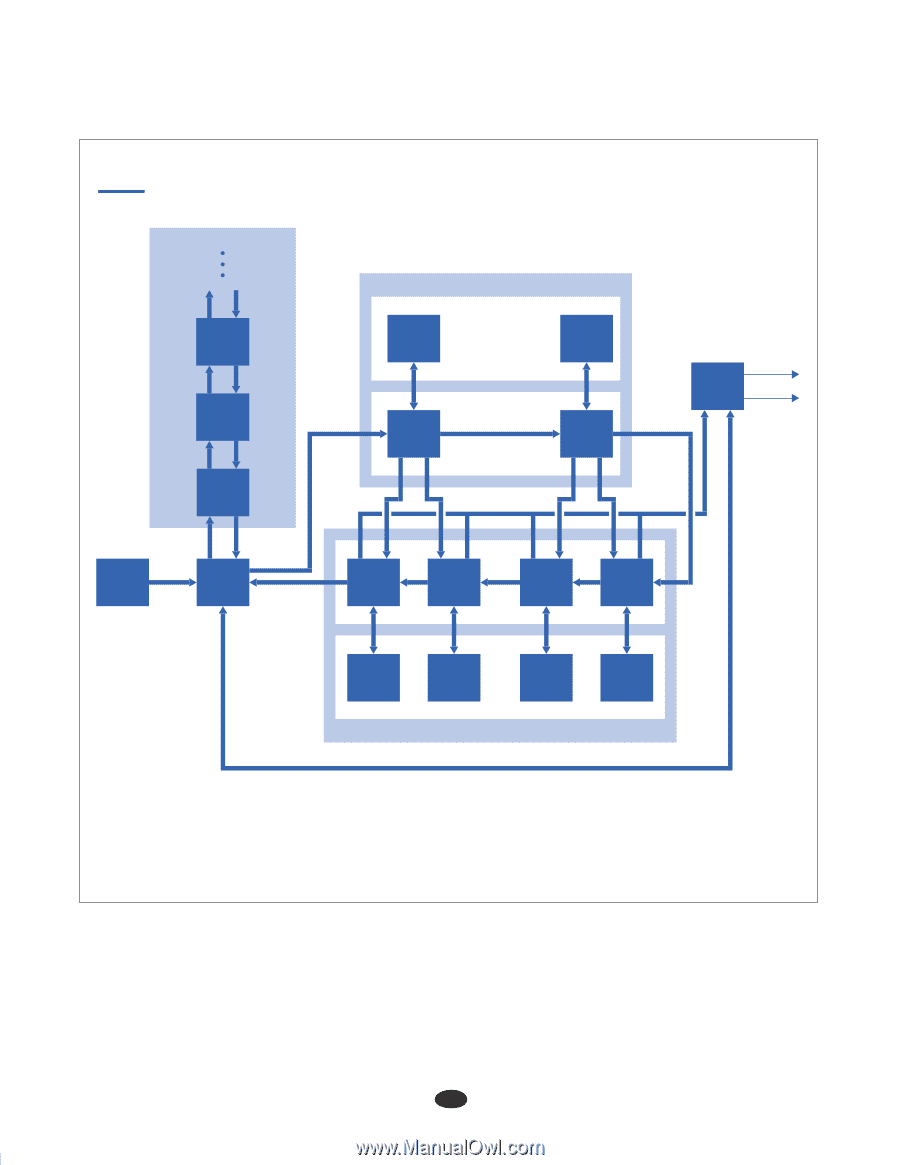
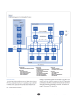
design of the buffering and the interface to the PCI. As
 |
View all HP Visualize b2000 manuals
Add to My Manuals
Save this manual to your list of manuals |
Page 2 highlights
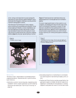
Figure 1 A chip-level diagram of the VISUALIZE fx6 product. Geometry Accelerator Up to 8 200 MHz/ 33 Bits 200 MHz/ 41 Bits Geometry Chip Texture Accelerator SDRAM Texture Cache RAM SDRAM Geometry Chip Geometry Chip Texture Chip 200 MHz/41 Bits Filtered Texture Data Texture Chip PCI2.1 66 MHz/ 64 Bits Interface Host Chip Raster Chip Raster Chip Raster Chip Raster Chip Video Refresh Data Video Chip RGB Video Data SGRAM SGRAM SGRAM SGRAM Rasterizer Frame Buffer RAM Video Control Bus Geometry Chip • 3D Geometry and Lighting Acceleration Texture Chip • Texture Rasterization • Texture Map Cache Controller • Texture Memory Control • Texture Interpolation Interface Chip • I/O Buffering • 3D Geometry Workload Distribution and Concentration • 2D and 3D Data Path Arbitration • 2D Acceleration • YUV to RGB Conversion Support • Pixel Level Pan and Zoom • Pixel Level Image Rotations Raster Chip • Fragment Processing • Frame Buffer Control Functions Video Chip • Color Lookup Tables • Video Timing • Digital-to-Analog Conversion • Video-Out Data Interface Chip The interface chip provides a PCI 2.1 (also referred to as PCI 2X) compliant interface.* It operates at up to 66 MHz in 64-bit mode. Special efforts have been made in the * PCI + Peripheral Component Interconnect. design of the buffering and the interface to the PCI. As a result, the driver is able to sustain writes of 3D geometry commands to the PCI at almost the theoretical maximum rates that could be computed for the PCI. The article on page 51 discusses PCI capability. Article 4 • © 1998 Hewlett Packard Company 29 May 1998 • The Hewlett-Packard Journal
-
 1
1 -
 2
2 -
 3
3 -
 4
4 -
 5
5 -
 6
6 -
 7
7
 |
 |