LG M6100 Service Manual - Page 28
AD6527B Architecture - software
 |
View all LG M6100 manuals
Add to My Manuals
Save this manual to your list of manuals |
Page 28 highlights
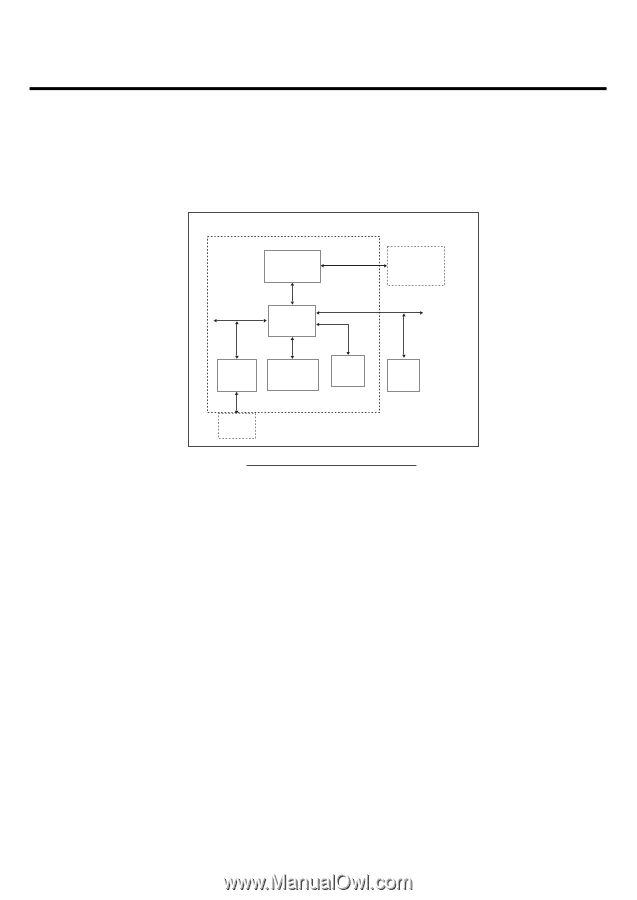
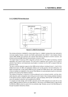
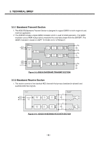
3. TECHNICAL BRIEF 3.4.2 AD6527B Architecture AD6527/AD6527B DSP Subsystem Serial Link DSP BUS PBUS DMA and BUS ARBITRATION RBUS IM Peripheral Subsystem SBUS MUC Subsystem (ARM7TDMI®) SRAM AD6535 Audio Baseband and Power Management EBUS FLASH RF-Control MMI USC Figure 3-7. AD6527B Architecture The internal architecture of AD6527B is shown above Figure 3-7. AD6527 regroups three main subsystems connected together through a dynamic and flexible communication bus network. It also includes onboard system RAM (SRAM) and interfaces with external Flash Memory, Baseband converter functions, and terminal functions like MMI, SIM and Universal System Connector (USC). The Digital Signal Processing (DSP) subsystem primarily hosts all the speech processing, channel equalization and channel codec functions. The code used to implement such functions can be stored in external Flash Memory and dynamically downloaded on demand into the DSP's program RAM and Instruction Cache. The micro-controller subsystem supports all the GSM terminal software, including the layer 1, 2 and 3 of the GSM protocol stack, the MMI, and applications software such as data services, test and maintenance. It is tightly associated with on-chip system SRAM and also includes boot ROM memory with a small dedicated routine to facilitate the initialization of the external Flash Memory via code download using the on-chip serial interface to the external Flash Memory interface. The peripheral subsystem is composed of system peripherals such as interrupt controller, real time clock, watch dog timer, power management and a timing and control module. It also includes peripheral interfaces to the terminal functions: keyboard, battery supervision, radio and display. Both the DSP and the MCU can access the peripheral subsystem via the peripheral bus (PBUS). For program and data storage, both the MCU subsystem and the DSP subsystem can access the on chip system SRAM and external memory such Flash Memory. The access to the SRAM module is made through the RAM Bus (RBUS) under the control of the bus arbitration logic. Similarly, access to the Flash Memory is through the parallel External Bus (EBUS). - 29 -
-
 1
1 -
2
-
3
-
4
-
5
-
6
-
7
-
8
-
9
-
10
-
11
-
12
-
13
-
14
-
15
-
16
-
17
-
18
-
19
-
20
-
21
-
22
-
 23
23 -
 24
24 -
 25
25 -
 26
26 -
 27
27 -
 28
28 -
 29
29 -
 30
30 -
 31
31 -
 32
32 -
 33
33 -
34
-
35
-
36
-
37
-
38
-
39
-
40
-
41
-
42
-
43
-
44
-
45
-
46
-
47
-
48
-
49
-
50
-
51
-
52
-
53
-
54
-
55
-
56
-
57
-
58
-
59
-
60
-
61
-
62
-
63
-
64
-
65
-
66
-
67
-
68
-
69
-
70
-
71
-
72
-
73
-
74
-
75
-
76
-
77
-
78
-
79
-
80
-
81
-
82
-
83
-
84
-
85
-
86
-
87
-
88
-
89
-
90
-
91
-
92
-
93
-
94
-
95
-
96
-
97
-
98
-
99
-
100
-
101
-
102
-
103
-
104
-
105
-
106
-
107
-
108
-
109
-
110
-
111
-
112
-
113
-
114
-
115
-
116
-
117
-
118
-
119
-
120
-
121
-
122
-
123
-
124
-
125
-
126
-
127
-
128
-
129
-
130
-
131
-
132
-
133
-
134
-
135
-
136
-
137
-
138
-
139
-
140
-
141
-
142
-
143
-
144
-
145
-
146
-
147
-
148
-
149
-
150
-
151
-
152
-
153
-
154
-
155
-
156
-
157
-
158
-
159
-
160
 |
 |