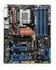
MSI Eclipse SLI User Guide - Page 71
MS-7520 Mainboard, Advance DRAM Configuration, 1N/2N Memory Timing, CAS# Latency CL, Advance Memory
 |
UPC - 816909051643
View all MSI Eclipse SLI manuals
Add to My Manuals
Save this manual to your list of manuals |
Page 71 highlights
MS-7520 Mainboard Advance DRAM Configuration Press to enter the sub-menu and the following screen appears. 1N/2N M emory Timing This item controls the SDRAM command rate. Select [1N] makes SDRAM signal controller to run at 1N (N=clock cycles) rate. Selecting [2N] makes SDRAM signal controller run at 2N rate. CAS# Latency (CL) This controls the CAS latency, which determines the timing delay (in clock cycles) before SDRAM starts a read command after receiving it. tRCD W hen DRAM is refreshed, both rows and columns are addressed separately. This setup item allows you to determine the timing of the transition from RAS (row address strobe) to CAS (column address strobe). The less the clock cycles, the faster the DRAM performance. tRP This setting controls the number of cycles for Row Address Strobe (RAS) to be allowed to precharge. If insufficient time is allowed for the RAS to accumulate its charge before DRAM refresh, refresh may be incomplete and DRAM may fail to retain data. This item applies only when synchronous DRAM is installed in the system. tRAS This setting determines the time RAS takes to read from and write to memory cell. Advance Memory Setting Setting to [Auto] enables the advance memory timing automatically to be determined by BIOS. Setting to [Manual] allows you to set advanced memory timings. Extreme Memory Profile This item is used to enable/disable the Intel Extreme Memory Profile (XMP). For further information please refer to Intel's official website. Memory Ratio This item allows you to set the memory multiplier. 3-24
-
 1
1 -
2
-
3
-
4
-
5
-
6
-
7
-
8
-
9
-
10
-
11
-
12
-
13
-
14
-
15
-
16
-
17
-
18
-
19
-
20
-
21
-
22
-
23
-
24
-
25
-
26
-
27
-
28
-
29
-
30
-
31
-
32
-
33
-
34
-
35
-
36
-
37
-
38
-
39
-
40
-
41
-
42
-
43
-
44
-
45
-
46
-
47
-
48
-
49
-
50
-
51
-
52
-
53
-
54
-
55
-
56
-
57
-
58
-
59
-
60
-
61
-
62
-
63
-
64
-
65
-
 66
66 -
 67
67 -
 68
68 -
 69
69 -
 70
70 -
 71
71 -
 72
72 -
 73
73 -
 74
74 -
 75
75 -
 76
76 -
77
-
78
-
79
-
80
-
81
-
82
-
83
-
84
-
85
-
86
-
87
-
88
-
89
-
90
-
91
-
92
-
93
-
94
-
95
-
96
-
97
-
98
-
99
-
100
-
101
-
102
-
103
-
104
-
105
-
106
-
107
-
108
-
109
-
110
-
111
-
112
-
113
-
114
-
115
-
116
-
117
-
118
-
119
-
120
-
121
-
122
-
123
-
124
-
125
-
126
-
127
-
128
-
129
-
130
-
131
-
132
-
133
-
134
-
135
-
136
-
137
-
138
-
139
-
140
-
141
-
142
-
143
-
144
-
145
-
146
-
147
-
148
-
149
-
150
-
151
-
152
-
153
-
154
-
155
-
156
-
157
-
158
 |
 |
