Pioneer GM-7150M Service Manual - Page 12
Schematic Diagram
 |
UPC - 012562725604
View all Pioneer GM-7150M manuals
Add to My Manuals
Save this manual to your list of manuals |
Page 12 highlights
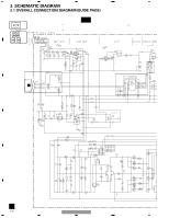
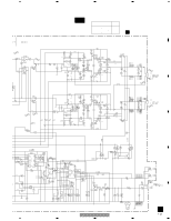
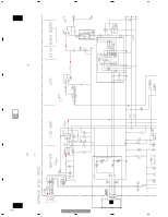
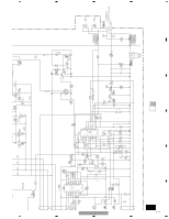
1 2 3 4 3. SCHEMATIC DIAGRAM 3.1 OVERALL CONNECTION DIAGRAM(GUIDE PAGE) Note: When ordering service parts, be sure to refer to " EXPLODED VIEWS AND PARTS LIST" or "ELECTRICAL PARTS LIST". A Large size A-a A-b SCH diagram A-a A-b Guide page A-a NOTE : Symbol indicates a resistor. No differentiation is made between chip resistors and discrete resistors. Symbol indicates a capacitor. No differentiation is made between chip capacitors and discrete capacitors. ← ← Decimal points for resistor and capacitor fixed values are expressed as : 2.2 2R2 0.022 R022 The > mark found on some component parts indicate the importance of the safety factor of the part. Therefore, when replacing, be sure to use parts of identical designation. A-a A-b Detailed page B 0dB +18.5dBs (BB ON INPUT MAX) 0dB +18.3dBs +17.5dBs LPF 0dB -1.7dB ~ -32.0dB 0dB or +12dB or +6dB ( or +9 +17.5dBs -15dBs B GAIN A BASS BOOST A B CN1351 C -0.8dB D E F A 12 GM-7100M/XU/EW 1 2 3 4
-
 1
1 -
2
-
3
-
4
-
5
-
6
-
 7
7 -
 8
8 -
 9
9 -
 10
10 -
 11
11 -
 12
12 -
 13
13 -
 14
14 -
 15
15 -
 16
16 -
 17
17 -
18
-
19
-
20
-
21
-
22
-
23
-
24
-
25
-
26
-
27
-
28
-
29
-
30
-
31
-
32
 |
 |
