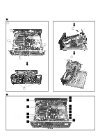
Pioneer VSX-D407 Service Manual - Page 50
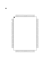
Pin Function - vsx d409 remote
 |
View all Pioneer VSX-D407 manuals
Add to My Manuals
Save this manual to your list of manuals |
Page 50 highlights
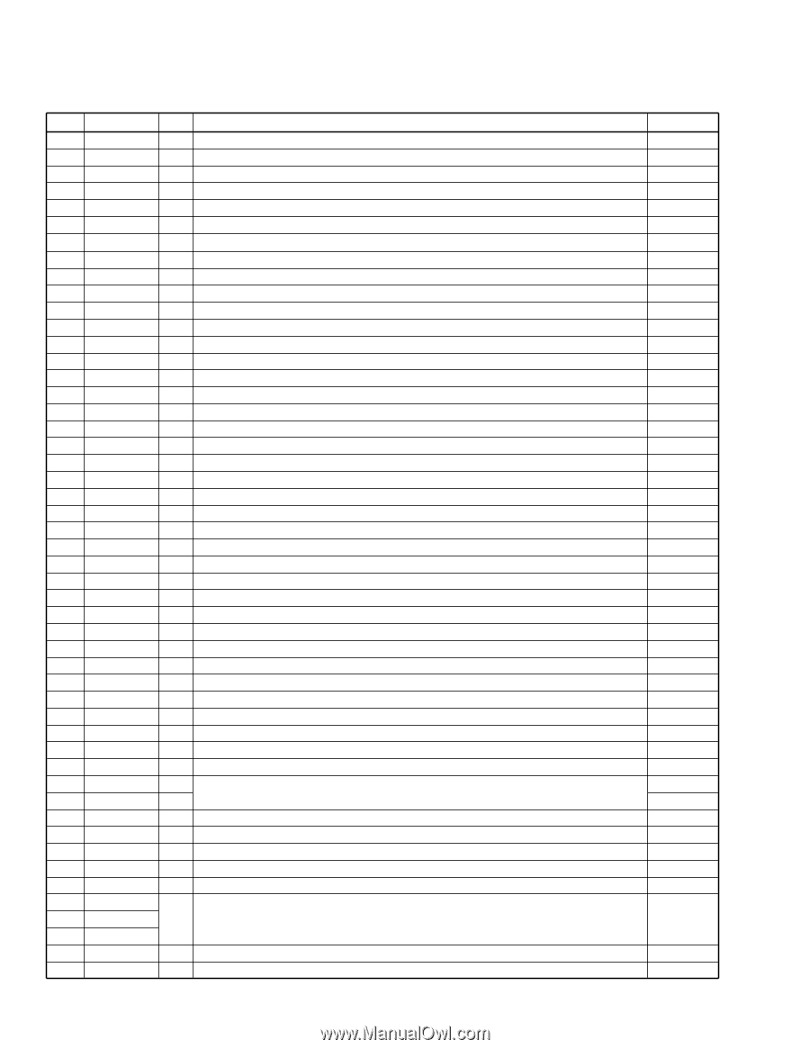
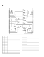
VSX-D409, VSX-D309 • Pin Function No. Pin Name 1 G2 2 G1 3 NC 4 ACIN 5 RDS_DT 6 RDS_CK 7 DIRLOCK 8 RMC 9 MRIN 10 PLL_CE 11 CDC_CS 12 CDC_CK 13 CDC_DO 14 CDC_DI 15 STEREO 16 TUNED 17 ENC_A 18 ENC_B 19 AMUTE 20 CSB 21 DSP_CS 22 DSP_CK 23 DSP_SI 24 DSP_SO 25 VER_2 26 ST_EVR 27 PLL_DO 28 AVref 29 KEYIN1 30 KEYIN2 31 KEYIN3 32 KEYIN4 33 VER 1 34 AMP_DC 35 AMP_OL 36 MVRATT 37 AVSS 38 RST 39 EXTAL 40 XTAL 41 VSS 42 TX 43 TEX 44 VDD 45 VFDP 46 VIDEO1 47 VIDEO2 48 VIDEO3 49 SYS_DT 50 SYS_CK I/O Pin Function O Grid output 2 O Grid output 1 − Connect to VDD I AC pulse input I Serial control DATA signal of RDS communication I Serial control CLOCK signal of RDS communication I ERR/OVER input from CODEC I Remote control signal input (no-carrier signal) I MULTI-ROOM input O Chip select signal for communication with LC72131 (tuner) O CODEC chip serect O CODEC, TC9164 control clock O CODEC, TC9164 control data output I Data input from CODEC I Stereo/Monoral signal judgment signal I TUNED information I Rotary encoder signal input A I Rotary encoder signal input B O Audio mute O Chip select for control of YSS912 sub DSP O Chip select for control of YSS912 main DSP O Clock signal for communication with YSS912 I DATA input for communication with YSS912 O DATA output signal for communication with YSS912 I Destination switch 2 O Strobe signal for communication with electric volume IC I Data input signal for communication with LC72131 (tuner) − Connect to VDD I Key input A/D conversion port 1 I Key input A/D conversion port 2 I Key input A/D conversion port 3 I Key input A/D conversion port 4 I Destination switch (A/D input) I DC abnormality detection of protection circuit (L : Abnormality detection) I Over-load detection of protection circuit (L : Abnormality detection) O ATT control of master volume (L : Less than -15dB) − Connect to VSS − Reset − Connect to the oscillator (7.2MHz) − − Connect to VSS − Open − Connect to VSS − +5V − -30V O NJM2296D control O Data signal for communication with M62446, TC9163, TC9164 and PLL O Clock signal for communication with M62446, TC9163, TC9164 and PLL 50 Active H H H L L L H H H L L H H H H
-
 1
1 -
2
-
3
-
4
-
5
-
6
-
7
-
8
-
9
-
10
-
11
-
12
-
13
-
14
-
15
-
16
-
17
-
18
-
19
-
20
-
21
-
22
-
23
-
24
-
25
-
26
-
27
-
28
-
29
-
30
-
31
-
32
-
33
-
34
-
35
-
36
-
37
-
38
-
39
-
40
-
41
-
42
-
43
-
44
-
 45
45 -
 46
46 -
 47
47 -
 48
48 -
 49
49 -
 50
50 -
 51
51 -
 52
52 -
 53
53 -
 54
54 -
 55
55 -
56
-
57
-
58
-
59
-
60
-
61
 |
 |