Polaroid FLM-3201 Service Manual - Page 14
IC block diagram - tv
 |
View all Polaroid FLM-3201 manuals
Add to My Manuals
Save this manual to your list of manuals |
Page 14 highlights
IC block diagram 1.MSP3420 Pins description: 2,3 PIN: SCL,SDA applied for control the operation of IC . 27,28 PIN: output left and right sound channel R/L to speaker processor. 36,37 PIN:AV OUT of sound R/L. 47,48 PIN:D4-1/D4-2/PCMCIA selected input R/L. 50,51 PIN:Input of VGA. R/L 53,54 PIN:Input of AV1/SVHS and AV2 R/L. 56,57 PIN:Input R/L of BS 67 PIN: Input TV SIF. 11
-
 1
1 -
2
-
3
-
4
-
5
-
6
-
7
-
8
-
 9
9 -
 10
10 -
 11
11 -
 12
12 -
 13
13 -
 14
14 -
 15
15 -
 16
16 -
 17
17 -
 18
18 -
 19
19 -
20
-
21
-
22
-
23
-
24
-
25
-
26
-
27
-
28
-
29
-
30
-
31
-
32
-
33
-
34
-
35
-
36
-
37
-
38
-
39
-
40
-
41
-
42
-
43
-
44
 |
 |

1
1
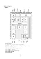
IC block diagram
1.MSP3420
Pins description:
2,3 PIN: SCL,SDA applied for control the operation of IC .
27,28 PIN: output left and right sound channel R/L to speaker processor.
36,37 PIN:AV OUT of sound R/L.
47,48 PIN:D4-1/D4-2/PCMCIA selected input R/L.
50,51 PIN:Input of VGA. R/L
53,54 PIN:Input of AV1/SVHS and AV2 R/L.
56,57 PIN:Input R/L of BS
67 PIN: Input TV SIF.