SanDisk SDCFB-128-A10 Product Manual - Page 43
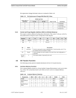
I/O Transfer Function
 |
UPC - 619659015213
View all SanDisk SDCFB-128-A10 manuals
Add to My Manuals
Save this manual to your list of manuals |
Page 43 highlights
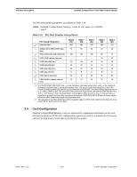
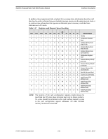
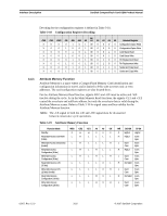
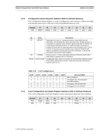
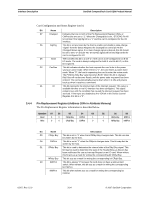
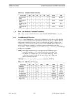
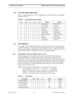
SanDisk CompactFlash Card OEM Product Manual Interface Description Pin replacement changed bit/mask values are contained in Table 3-21. Table 3-21 Pin Replacement Changed Bit/Mask Bit Values Initial Value of (C) Status 0 1 X X Written by Host "C" Bit X X 0 1 "M" Bit 0 0 1 1 Final "C" Bit 0 1 0 1 Comments Unchanged Unchanged Cleared by host Set by host 3.4.5 Socket and Copy Register (Address 206h in Attribute Memory) This register contains additional configuration information. This register is always written by the system before writing the card's Configuration Index Register. Operation D7 D6 D5 Read Reserved 0 0 Write 0 0 0 D4 Drive# Drive# (0) D3 D2 D1 D0 0 0 0 0 X X X X Bit D7 D4 D3-D0 (write) Name Reserved Drive# X Description This bit is reserved for future standardization. This bit must be set to "0" by the software when the register is written. This bit indicates the drive number of the card if twin card configuration is supported. The socket number is ignored by the card. 3.5 I/O Transfer Function The following sections provide valuable information for the I/O Transfer function. 3.5.1 Common Memory Function The Common Memory transfer to or from SanDisk CompactFlash memory cards can be either 8 or 16 bits. The card permits both 8- and 16-bit accesses to all of its Common Memory addresses. Table 3-22 Common Memory Function Function Code Standby Byte Read Access (8 bits) Byte Write Access (8 bits) -REG -CE2 -CE1 A0 -OE -WE D15-D8 X H H X X X High Z H H L L L H High Z H H L H L H High Z H H L L H L Don't Care H H L H H L Don't Care D7-D0 High Z Even Byte Odd Byte Even Byte Odd Byte © 2007 SanDisk Corporation 3-25 Rev. 12.0, 02/07
-
 1
1 -
2
-
3
-
4
-
5
-
6
-
7
-
8
-
9
-
10
-
11
-
12
-
13
-
14
-
15
-
16
-
17
-
18
-
19
-
20
-
21
-
22
-
23
-
24
-
25
-
26
-
27
-
28
-
29
-
30
-
31
-
32
-
33
-
34
-
35
-
36
-
37
-
 38
38 -
 39
39 -
 40
40 -
 41
41 -
 42
42 -
 43
43 -
 44
44 -
 45
45 -
 46
46 -
 47
47 -
 48
48 -
49
-
50
-
51
-
52
-
53
-
54
-
55
-
56
-
57
-
58
-
59
-
60
-
61
-
62
-
63
-
64
-
65
-
66
-
67
-
68
-
69
-
70
-
71
-
72
-
73
-
74
-
75
-
76
-
77
-
78
-
79
-
80
-
81
-
82
-
83
-
84
-
85
-
86
-
87
-
88
-
89
-
90
-
91
-
92
-
93
-
94
-
95
-
96
-
97
-
98
-
99
-
100
-
101
-
102
-
103
-
104
-
105
-
106
-
107
-
108
 |
 |