SanDisk SDCFRX4-4096-902 Product Manual - Page 35
Table 3-14, I/O Write Timing Specification, De-skewing., Transfer Timing., Register Transfers
 |
UPC - 619659027988
View all SanDisk SDCFRX4-4096-902 manuals
Add to My Manuals
Save this manual to your list of manuals |
Page 35 highlights
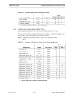
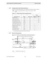
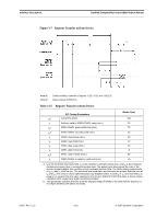
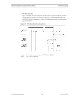
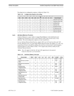
SanDisk CompactFlash Card OEM Product Manual Interface Description Table 3-14 contains the specification information related to the I/O Write Timing Diagram. Table 3-14 I/O Write Timing Specification Item Data Setup before -IOWR Data Hold following -IOWR -IOWR Width Time Address Setup before -IOWR Address Hold following -IOWR -CE Setup before -IOWR -CE Hold following -IOWR -REG Setup before -IOWR -REG Hold following -IOWR -IOIS16 Delay falling from Address -IOIS16 Delay rising from -IORD -IOIS16 Delay falling from Address -IOIS16 Delay rising from Address Symbol tsu (IOWR) th (IOWR) tw (IOWR) tsuA(IOWR) thA(IOWR) tsuCE(IOWR) thCE(IOWR) tsuREG(IOWR) thREG(IOWR) tdfIOIS16(ADR) tdr-IOIS16(ADR) tdfIOIS16(ADR) tdrIOIS16(ADR) IEEE Symbol tDVIWL tWHDX tlWLIWH tAVIWL tlWHAX tELIWL tlWHEH tRGLIWL tlWHRGH tAVISL tAVISH tAVISL tAVISH a. The maximum load on -IOIS16 is 1 LSTTL with 50 pF total load. Min. (ns) 60 30 165 70 20 5 20 5 0 --------- Max. (ns 35a 35 35 35 3.3.10 True IDE Mode The following sections provide valuable information for the True IDE mode. De-skewing. The host will provide cable de-skewing for all signals originating from the device. The device will provide cable de-skewing for all signals originating at the host. All timing values and diagrams are shown and measured at the connector of the selected device. Transfer Timing. The minimum cycle time supported by devices in PIO Mode 3, 4 and Multiword DMA Mode 1, 2 respectively will always be greater than or equal to the minimum cycle time defined by the associated mode (e.g., a device supporting PIO Mode 4 timing will not report a value less than 120 ns. The minimum cycle time defined for PIO mode 4 timings). • Register Transfers Figure 3-7 defines the relationships between the interface signals for register transfers. For PIO Modes 3 and above, the minimum value of t0 is specified by Word 68 in the IDENTIFY DEVICE parameter list. Table 3-15 defines the minimum value that will be placed in Word 68. In Figure 3-7, all signals shown with the asserted condition facing the top of the page. The negated condition is shown toward the bottom of the page relative to the asserted condi tion. NOTE: SanDisk CompactFlash Memory cards do not assert an -IORDY signal. © 2007 SanDisk Corporation 3-17 Rev. 12.0, 02/07
-
 1
1 -
2
-
3
-
4
-
5
-
6
-
7
-
8
-
9
-
10
-
11
-
12
-
13
-
14
-
15
-
16
-
17
-
18
-
19
-
20
-
21
-
22
-
23
-
24
-
25
-
26
-
27
-
28
-
29
-
 30
30 -
 31
31 -
 32
32 -
 33
33 -
 34
34 -
 35
35 -
 36
36 -
 37
37 -
 38
38 -
 39
39 -
 40
40 -
41
-
42
-
43
-
44
-
45
-
46
-
47
-
48
-
49
-
50
-
51
-
52
-
53
-
54
-
55
-
56
-
57
-
58
-
59
-
60
-
61
-
62
-
63
-
64
-
65
-
66
-
67
-
68
-
69
-
70
-
71
-
72
-
73
-
74
-
75
-
76
-
77
-
78
-
79
-
80
-
81
-
82
-
83
-
84
-
85
-
86
-
87
-
88
-
89
-
90
-
91
-
92
-
93
-
94
-
95
-
96
-
97
-
98
-
99
-
100
-
101
-
102
-
103
-
104
-
105
-
106
-
107
-
108
 |
 |