SanDisk SDSDQ4096A11M Product Manual - Page 17
microSD Card Product Family Registers
 |
UPC - 619659033507
View all SanDisk SDSDQ4096A11M manuals
Add to My Manuals
Save this manual to your list of manuals |
Page 17 highlights
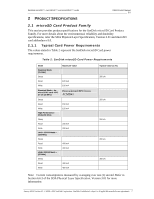
SanDisk microSD™, microSDHC™ and microSDXC™ cards Card VDD OEM Product Manual 2.5 Figure 6: Recommended Power Control Scheme The recommended power control scheme for SanDisk microSD cards is illustrated in Figure 6. Most card connectors have a card detect switch that signals the SD host when the card is inserted. After the host is aware of the card insertion, it turns on the FET switch to apply power to card's VDD pin. Once the card is inserted and all card pins are making contact, there should be a delay before the FET switch is turned on. Note: Because there are clamping diodes on the CMD, CLK, and DAT0-3 pins, it is crucial to ensure that CLK, CMD, and DAT0-3 are at zero (0) volts during the delay and before the FET switch is turned on. If any I/O pin, (CMD, CLK, or DAT0-3) goes above zero volts during the delay and before power reaches the card VDD pin, it will forward bias the clamping diodes and can cause the card to go into an unknown state. It is the host's responsibility to make sure power gets to VDD before CMD, CLK, or DAT0-3 go above zero volts. 3.4.2 Bus Operating Conditions SPI Mode bus operating conditions are identical to SD Card Bus Mode operating conditions. For details, see Section 6.6 of the SDA Physical Layer Specification, Version 3.01. 3.4.3 Bus Timing See SDA Physical Layer Specification, Version 3.01. 3.5 microSD Card Product Family Registers There is a set of eight registers within the card interface. However, the DSR Register is optional and is not used in the SanDisk microSD Card Product Family. For specific information about all registers, refer to Section 5 of the SDA Physical Layer Specification, Version 3.01. 3.5.1 Operation Conditions Register The Operation Conditions Register (OCR) stores a card's VDD voltage profile. Refer to Section 5.1 of the SDA Physical Layer Specification, Version 3.01 for more information. 3.5.2 Card Identification Register The Card Identification (CID) Register is 16 bytes long and contains the unique card identification number. It is programmed during card manufacturing and cannot be changed by card hosts. See Table 8. January 2012 Version 2.5 © 2008 - 2012 SanDisk Corporation. SanDisk Confidential, subject to all applicable non-disclosure agreements 12
-
 1
1 -
2
-
3
-
4
-
5
-
6
-
7
-
8
-
9
-
10
-
11
-
 12
12 -
 13
13 -
 14
14 -
 15
15 -
 16
16 -
 17
17 -
 18
18 -
 19
19 -
 20
20 -
 21
21 -
 22
22 -
23
-
24
-
25
-
26
 |
 |
