Sony SA-WP16 Service Manual - Page 3
Sa-wp16, Diagrams
 |
View all Sony SA-WP16 manuals
Add to My Manuals
Save this manual to your list of manuals |
Page 3 highlights
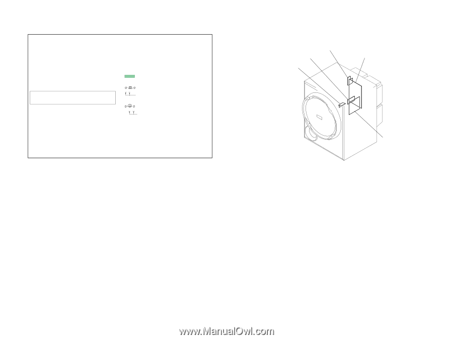
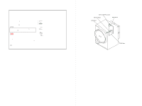
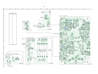
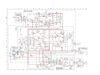
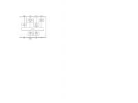
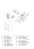
SECTION 1 DIAGRAMS • NOTE FOR PRINTED WIRING BOARDS AND SCHEMATIC DIAGRAMS THIS NOTE IS COMMON FOR PRINTED WIRING BOARDS AND SCHEMATIC DIAGRAMS. (In addition to this, the necessary note is printed in each block.) For schematic diagrams. Note: • All capacitors are in µF unless otherwise noted. (p: pF) 50 WV or less are not indicated except for electrolytics and tantalums. • All resistors are in Ω and 1/4 W or less unless otherwise specified. • C : panel designation. Note: The components identified by mark 0 or dotted line with mark 0 are critical for safety. Replace only with part number specified. • A : B+ Line. • B : B- Line. • Voltages and waveforms are dc with respect to ground under no-signal (detuned) conditions. no mark : Power on ∗ : Impossible to measure • Voltages are taken with a VOM (Input impedance 10 MΩ). Voltage variations may be noted due to normal production tolerances. • Signal path. F : AUDIO • Abbreviation E51: Chilean and Peruvian model For printed wiring boards. Note: • X : parts extracted from the component side. • a : Through hole. • : Pattern from the side which enables seeing. • Indication of transistor. BEC These are omitted BC E These are omitted • Abbreviation E51: Chilean and Peruvian model 1-1. CIRCUIT BOARDS LOCATION INPUT CONTROL board SWITCH board MAIN board LED board SA-WP16 Ver. 1.1 TRANS board SA-WP16 3 3
-
 1
1 -
 2
2 -
 3
3 -
 4
4 -
 5
5 -
 6
6 -
 7
7 -
 8
8 -
 9
9 -
10
-
11
-
12
 |
 |