Sony STR-DB830 Service Manual - Page 36
Ic1101, Lc89055w Digital Audio I/f Receiver Digital Board - receivers
 |
View all Sony STR-DB830 manuals
Add to My Manuals
Save this manual to your list of manuals |
Page 36 highlights
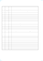
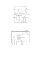
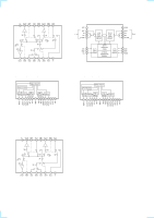
IC1101 LC89055W DIGITAL AUDIO I/F RECEIVER (DIGITAL BOARD) Pin No. Pin Name I/O Description 1 DISEL I Input data select. (connected to ground.) 2 DOUT O EIAJ data and parity flag output terminal (Not used) 3 DIN0 I Amplifier integrate data input terminal 4 DIN1 O Amplifier integrate data input terminal (Connecting to ground) 5 DIN2 I Amplifier integrate data input terminal (Connecting to ground) 6 D. GND - Digital ground 7 D. VDD O Digital power supply 8 R I Input terminal for VCO generator band adjustment 9 V IN I Input terminal for VCO self running frequency set 10 LPF O External LPF for PLL is connected to this terminal 11 A. VDD - Analog power supply 12 A. GND - Analog ground 13 CK OUT - 256fs or 128fs clock output terminal (Select CLKMD terminal) 14 BCK O Bit clock output terminal 15 LRCK O L, R clock output terminal (L-ch: "H", R-ch: "L") 16 DATA O O Audio data output terminal 17 XSTATE O Xtal status frag output. 18 D. GND - Digital ground 19 D. VDD - Digital power supply 20 XMCK - Not used. 21 XOUT O Crystal oscillator output terminal (Not used.) 22 XIN I Crystal oscillator input terminal 23 EMPHA O Emphasis monitor output terminal ("H" = ON) (Not used.) 24 AUDIO - Not used. 25 CSFLAG O C-bit change frag output. 26 F0/P0/C0 - Not used. 27 F1/P1/C1 - Not used. 28 F2/P2/C2 - Not used. 29 F3/P3/C3 - Not used. 30 D. VDD - Digital power supply 31 D. GND - Digital ground 32 AUTO O Non PCM data detect flag output. 33 BPSYNC O Non PCM sync detect flag output. 34 ERROR O Error mute output terminal 35 DO O Microprocessor I/F. When CCB/SUB is "H", data output terminal (high level open drain output) (Not used) 36 DI I Microprocessor I/F. Data input terminal 37 CE I Microprocessor I/F. Chip enable/latch input terminal 38 CLK I Microprocessor I/F. Clock input terminal 39 XSEL I Xtal select. (Connected to +5V.) 40 MODE0 I Mode 0 input. (Connected to ground.) 41 MODE1 I Mode 1 input. (Connected to ground.) 42 D. GND - Digital ground 43 D. VDD - Digital power supply 44 DOSEL0 O Output data select 0. (Connected to ground.) 45 DOSEL1 O Output data select 1. (Connected to ground.) 46 CKSEL0 I System clock select input 0. (Connected to ground.) 47 CKSEL1 I System clock select input 1. (Connected to ground.) 48 XMODE I Reset input. - 58 -
-
 1
1 -
2
-
3
-
4
-
5
-
6
-
7
-
8
-
9
-
10
-
11
-
12
-
13
-
14
-
15
-
16
-
17
-
18
-
19
-
20
-
21
-
22
-
23
-
24
-
25
-
26
-
27
-
28
-
29
-
30
-
 31
31 -
 32
32 -
 33
33 -
 34
34 -
 35
35 -
 36
36 -
 37
37 -
 38
38 -
 39
39 -
 40
40 -
 41
41 -
42
-
43
-
44
-
45
-
46
-
47
-
48
-
49
-
50
-
51
-
52
-
53
-
54
-
55
-
56
-
57
-
58
-
59
-
60
-
61
-
62
-
63
-
64
 |
 |
