Yamaha MCR-330 Service Manual - Page 39
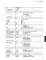
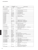
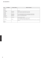
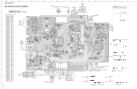
Port Name, Function Name, Detail of Function, Ground / Analog power supply for USB / Connect to VSS.
 |
UPC - 027108106274
View all Yamaha MCR-330 manuals
Add to My Manuals
Save this manual to your list of manuals |
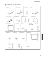
Page 39 highlights
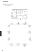
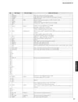
CRX-330/NS-BP100 No. Port Name 1 N.C. 2 USBNOC 3 USBNPP 4 USBD- 5 VSS 6 USBD+ 7 AVDD 8 N.C. 9 VDD3 10 VDDI 11 OSCI 12 OSCO 13 VSS 14 NRST 15 MMOD0 16 MMOD1 17 VPP 18 OCD_SDA 19 OCD_SCL 20 21 22 N.C. 23 24 25 USB_IN 26 27 28 29 30 31 N.C. 32 33 34 35 36 37 38 VDD3 39 N.C. 40 VSS 41 N.C. 42 VDDI 43 44 N.C. 45 46 I2C_SCL 47 N.C. 48 I2C_SDA 49 VDD3 Function Name Detail of Function AVSS USB over-current input (negative polarity) USB, VBUS power output control terminal (negative polarity) USB D- terminal Ground / Analog power supply for USB / Connect to VSS. USB D+ terminal Analog power supply for USB / Connect to VDD33. VDD33 VDD18/VOUT Power for on-chip regulator (2.7V to 3.6V) I/O power supply (2.7V to 3.6V) Power for internal circuit (1.8V t±0.15V) Connect all VDD18 terminals outside of chip. Also, connect a 10μF capacitor between VDD18 and VSS of No.10 pin and place it near LSI. On-chip regulator output (1.8V ±0.15V) High-speed oscillation input terminal (fosc) (When PLL used: 6.33 MHz to 20 MHz) High-speed oscillation output terminal Ground Reset signal input terminal (negative polarity) Operation mode setting terminal Operation mode setting terminal Power for rewriting built-in Flash memory (3.3V ±0.3V) / only for Flash built in model Clock, data input/output terminal for on-chip debugger Clock, data input/output terminal for on-chip debugger General purpose input/output port 0 VDD33 VDD18 P35/SCL3 P33/SDA3 VDD5 Power for on-chip regulator (2.7V to 3.6V) I/O power supply (2.7V to 3.6V) Ground Power supply for internal circuit (1.8V ±0.15V) Connect all VDD18 terminals outside of chip. Also, connect a 10μF capacitor between VDD18 and VSS of No.10 pin and place it near LSI. General purpose input/output port 3 General purpose input/output port 3 I/O power supply (5V type I/O 39 CRX-330/NS-BP100
-
 1
1 -
2
-
3
-
4
-
5
-
6
-
7
-
8
-
9
-
10
-
11
-
12
-
13
-
14
-
15
-
16
-
17
-
18
-
19
-
20
-
21
-
22
-
23
-
24
-
25
-
26
-
27
-
28
-
29
-
30
-
31
-
32
-
33
-
 34
34 -
 35
35 -
 36
36 -
 37
37 -
 38
38 -
 39
39 -
 40
40 -
 41
41 -
 42
42 -
 43
43 -
 44
44 -
45
-
46
-
47
-
48
-
49
-
50
-
51
-
52
-
53
-
54
-
55
-
56
-
57
-
58
-
59
-
60
-
61
-
62
-
63
-
64
-
65
-
66
-
67
-
68
-
69
-
70
 |
 |