ASRock P4i45D User Manual - Page 11
Jumpers Setup, 8 Connectors
 |
View all ASRock P4i45D manuals
Add to My Manuals
Save this manual to your list of manuals |
Page 11 highlights
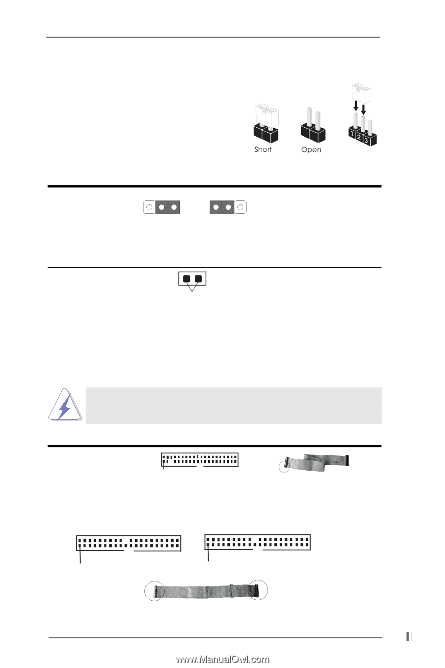
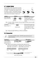
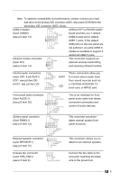
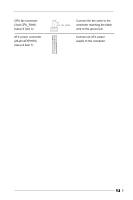
2.7 Jumpers Setup The illustration shows how jumpers are setup. When the jumper cap is placed on pins, the jumper is "SHORT". If no jumper cap is placed on pins, the jumper is "OPEN". The illustration shows a 3-pin jumper whose pin1 and pin2 are "SHORT" when jumper cap is placed on these 2 pins. Jumper Setting Description PS2_USB_PWR1 2_3 1_2 Short pin2, pin3 to set at (see p.6 item 22) +5VSB (standby) and +5VSB (Default) +5V enable PS/2 or USB wake up events. Note: To select +5VSB, it requires 2 Amp and higher standby current provided by power supply. CLRCMOS1 Disconnect the power cord, (see p.6 item 17) then short the solder points solder points to clear CMOS by using metal material, e.g., a paper clip. Note: There are SOLER POINTS but no PINS on CLRCMOS1. 2.8 Connectors Connectors are NOT jumpers. DO NOT place jumper caps over these connectors. Connector Figure Description FDD connector (33-pin FLOPPY1) (see p.6 item 10) Pin1 FLOPPY1 Red marking Note: Match the red marking on the floppy ribbon cable with Pin1. Primary IDE connector (Blue) Secondary IDE connector (Black) (39-pin IDE1, see p.6 item 7) (39-pin IDE2, see p.6 item 8) PIN1 IDE1 PIN1 IDE2 Connect this BLUE end to the motherboard 80-Pin ATA 100 cable Connect this BLACK end to the IDE devices 11
-
 1
1 -
2
-
3
-
4
-
5
-
 6
6 -
 7
7 -
 8
8 -
 9
9 -
 10
10 -
 11
11 -
 12
12 -
 13
13 -
 14
14 -
 15
15 -
 16
16 -
17
-
18
-
19
-
20
-
21
-
22
-
23
-
24
 |
 |