Asus TX97-N TX97-N User Manual - Page 42
Onboard FDC Swap A & B No Swap
 |
View all Asus TX97-N manuals
Add to My Manuals
Save this manual to your list of manuals |
Page 42 highlights
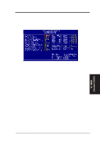
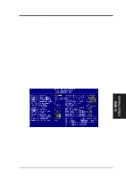
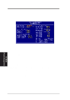
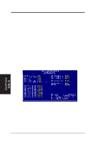
IV. BIOS SOFTWARE SDRAM CAS# Latency (3T) If you use ASUS SDRAM DIMM modules, you can set this to 2T for better performance, otherwise leave on default or check with your vendor for DIMM specs. SDRAM Speculative Read (Disabled) If Enabled, the CPU will issue predict commands to access the DRAM, if a miss occurs, the CPU will cancel this command. Some operating systems under certain situations have a problem utilizing this feature so it is normally Disabled. Passive Release (Enabled) This is a mechanism that allows concurrency of ISA/EISA cycles and CPU-to-PCI cycles. When this feature is enabled, the TXC will be possible to re-arbitrate PCI bus and allow the CPU to access PCI even when the PCEB has been granted the bus. Delayed Transaction (Disabled) If Enabled, this frees the PCI Bus during CPU accessing of 8-bit ISA cards which normally consume about 50-60 PCI Clocks without PCI delayed transaction. If PCI Bus Masters cannot use the PCI Bus, leave this on the default setting of Disabled for some ISA cards that are not PCI 2.1 compliant. 16-bit I/O Recovery Time (1 BUSCLK) Timing for 16-bit ISA cards. 8-bit I/O Recovery Time (1 BUSCLK) Timing for 8-bit ISA cards. Video BIOS Cacheable (Enabled) Allows the Video BIOS to be cached to allow faster execution. Leave on default setting of Enabled for better performance, otherwise Disabled. Memory Hole at Address (None) This features reserves either 14MB-16MB or 15MB-16MB memory address space to ISA expansion cards that specifically require this setting. Memory from 14MB and up or 15MB and up will be unavailable to the system because expansion cards can only access memory up to 16MB...Onboard FDC Controller (Enabled) When enabled, this field allows you to connect your floppy disk drives to the onboard floppy drive connector instead of a separate controller card. If you want to use a different controller card to connect the floppy drives, set this field to Disabled. Onboard FDC Swap A & B (No Swap) This field allows you to reverse the hardware drive letter assignments of your floppy disk drives. Two options are available: Swap AB and No Swap (default). If you want to switch drive letter assignments, set this field to Swap AB, and the swap will be controlled by the onboard chipset. IV. BIOS (Chipset Features) 42 ASUS TX97-N User's Manual
-
 1
1 -
2
-
3
-
4
-
5
-
6
-
7
-
8
-
9
-
10
-
11
-
12
-
13
-
14
-
15
-
16
-
17
-
18
-
19
-
20
-
21
-
22
-
23
-
24
-
25
-
26
-
27
-
28
-
29
-
30
-
31
-
32
-
33
-
34
-
35
-
36
-
 37
37 -
 38
38 -
 39
39 -
 40
40 -
 41
41 -
 42
42 -
 43
43 -
 44
44 -
 45
45 -
 46
46 -
 47
47 -
48
-
49
-
50
-
51
-
52
-
53
-
54
-
55
-
56
-
57
-
58
-
59
-
60
 |
 |
