Compaq ProLiant 8500 ProLiant 8500 Server Technology - Page 6
Processor and I/O Buses, Memory Subsystem, Processor, address, Memory, Array, I/O bus - proliant 800
 |
View all Compaq ProLiant 8500 manuals
Add to My Manuals
Save this manual to your list of manuals |
Page 6 highlights
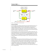
TC000604TB TECHNOLOGY BRIEF (cont.) ... Cache Accelerator Cache Accelerator Processor bus address Memory Access Controller (MAC) address address Processor bus A Memory Array D A Memory Array D data Data Interface Buffer (DIB) data I/O bus data address Figure 3: ASIC partitioning in the Profusion chipset. Processor and I/O Buses The ProLiant 8500 server includes two 64-bit processor buses and a dedicated 64-bit I/O bus. All three are 100-MHz advanced Gunning transceiver logic plus (AGTL+) buses with a theoretical maximum throughput of 800 MB/s. AGTL+ buses facilitate higher clock speeds without significantly reducing the bus length or number of electrical loads. Each 100-MHz AGTL+ bus can support a maximum of five loads per bus. This allows four processors and one connection to the memory controller on each processor bus. The use of two processor buses enables the ProLiant 8500 server to support up to eight Pentium III Xeon processors. The Profusion chipset joins the two processor buses, the I/O bus, and the two memory ports. The otherwise independent processor and I/O buses are joined by a logical connection that is made only when required to transfer data. Each of the three AGTL+ buses has independent access to the two memory ports. This architecture prevents I/O traffic from consuming bandwidth on the processor bus. In addition, the use of 100-MHz buses and five independent paths allows the crossbar switch to deliver an aggregate instantaneous peak throughput of 4 GB/s-unprecedented high performance for customers. Memory Subsystem The ProLiant 8500 memory subsystem includes dual 100-MHz buses, each with its own memory controller. The use of two memory buses increases memory bandwidth, reduces access conflicts, and increases the quantity of memory supported. Memory attached to each of the buses is cacheline interleaved, which means the buses share a common address range. One memory bus responds to even-numbered cache lines, and the other bus responds to odd-numbered cache lines. This configuration allows simultaneous use of both memory buses, which theoretically doubles throughput. It is especially advantageous for applications that access memory randomly. In random accesses, roughly half the requests at any one time are even-numbered lines, while the other half are odd-numbered lines. 6
-
 1
1 -
 2
2 -
 3
3 -
 4
4 -
 5
5 -
 6
6 -
 7
7 -
 8
8 -
 9
9 -
 10
10 -
 11
11 -
 12
12 -
13
-
14
-
15
-
16
-
17
-
18
-
19
-
20
-
21
-
22
-
23
 |
 |
