Foxconn A74MX-K English manual - Page 36
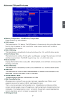
► Memory Configuration / DRAM Timing Configuration - video drivers
 |
View all Foxconn A74MX-K manuals
Add to My Manuals
Save this manual to your list of manuals |
Page 36 highlights
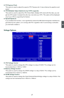
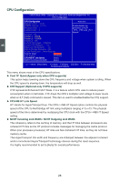
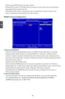
Advanced Chipset Features CMOS Setup Utility - Copyright (C) 1985-2006, American Megatrends, Inc. Advanced Chipset Features �N��o�r�t�h�b�r�id��g�e��C�h��ip�s��e�t�C��o�n�f�ig��u�r�a�ti�o�n� Help Item ► Memory Configuration [Press Enter] D�R�A��M��T�im��in�g��C�o�n��fi�g�u�ra�t�io�n� [Press Enter] CAS Latency :4.0 RAS/CAS Delay :6 ClK ���R�o�w��P�r�e�c�h�a�rg�e��T�i�m�e 4�C��lK ��M�in��A�ct�iv�e�R�A�S 2�3�C�lK� RAS/RAS Delay :4 ClK Row Cycle :15 ClK Internal Graphics Configuration �In�t�e�rn�a�l�G�r�a�p�h�ic�s�M��o�de E�n�a�b�le�d�] �U�M��A�F�r�a�m�e�B��u�ffe�r�S��iz�e A�u�to�] GFX Engine Clock [400]�� Surround View [Disabled] 3 Move Enter:Select +/-/:Value F10:Save ESC:Exit F1:General Help F9:Optimized Defaults ► Memory Configuration / DRAM Timing Configuration Press to go to its submenu. ► CAS Latency This item shows the CAS latency. The CAS Latency is the number of clock cycles that elapse from the time the request for data is sent to the actual memory location until the data is transmitted from the module. ► RAS / CAS Delay This item displays a delay time (in clock cycles) between the CAS and RAS strobe signals. ► Row Precharge Time This item shows the number of clock cycles taken between issuing of the precharge command and the active command. The DRAM row precharge time is in unit of clock cycle. ► Min Active RAS Displays the number of clock cycles taken between a bank active command and issuing of the precharge command. ► RAS / RAS Delay This item displays a delay time (in clock cycles) between the RAS and RAS strobe signals. ► Row Cycle This item shows the minimum timing interval between successive active commands to the same bank. The row cycle time is in unit of clock cycle. ► Internal Graphics Mode Enable/Disable the integrated UMA graphics controller. ► UMA Frame Buffer Size Allocates system memory for use as video memory to ensure the most efficient use of available resources for maximum 2D/3D graphics performance. This is a memory allocation method addition to the Unified Memory Architecture (UMA) concept, wherein a static amount of page-locked graphics memory is allocated during driver initialization. This fixed amount of memory will provide the user with a guaranteed graphics memory at all times, and will no longer be available to the OS. ► GFX Engine Clock 29
-
 1
1 -
2
-
3
-
4
-
5
-
6
-
7
-
8
-
9
-
10
-
11
-
12
-
13
-
14
-
15
-
16
-
17
-
18
-
19
-
20
-
21
-
22
-
23
-
24
-
25
-
26
-
27
-
28
-
29
-
30
-
 31
31 -
 32
32 -
 33
33 -
 34
34 -
 35
35 -
 36
36 -
 37
37 -
 38
38 -
 39
39 -
 40
40 -
 41
41 -
42
-
43
-
44
-
45
-
46
-
47
-
48
-
49
-
50
-
51
-
52
-
53
-
54
-
55
-
56
-
57
-
58
-
59
-
60
-
61
-
62
-
63
-
64
-
65
-
66
-
67
-
68
-
69
-
70
-
71
-
72
-
73
-
74
-
75
-
76
-
77
-
78
-
79
-
80
-
81
-
82
-
83
-
84
-
85
-
86
-
87
-
88
-
89
-
90
-
91
-
92
-
93
-
94
-
95
-
96
-
97
-
98
-
99
-
100
-
101
-
102
-
103
-
104
-
105
 |
 |
