Gigabyte GA-6TXSL Manual - Page 23
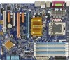
Block Diagram
 |
View all Gigabyte GA-6TXSL manuals
Add to My Manuals
Save this manual to your list of manuals |
Page 23 highlights
2-4: Block Diagram Block Diagram CLOCK GENERATOR CK505 INTEL LGA1366 core i7 1333/1066/800 VID0~5 VRD 11.1 PCI-E Graphic Card PCIE x16 Slot PCIE x4 Slot PCIE x8 Slot PCIE x8 Slot PCIE x16 PCIE x4 PCIE x8 PCIE x8 FSB IOH Intel X58 CHANNEL A DDR3 1066/1333 un-Buffered ECC/Non ECC/Reg ECC D/MMX2 CHANNEL B DDR3 1066/1333 un-Buffered ECC/Non ECC/Reg ECC D/MMX2 DMI_PN_0~3 DMI Control Bus PCI CHANNEL C DDR3 1066/1333 un-Buffered ECC/Non ECC/Reg ECC D/MMX2 IEEEE 1394a 1394 1394 TSB43AB23 USB USB USB Front Panel 1394 PCI 32/33MHz Slot SPI BUS SPI FWH 82801JR ICH10RAID USB LPC BUS USB x 2 SATA x 6 PCIE x1 USB Intel 82567LM Rear Panel RJ45 & USBx2 ITE 8720F USB x 2 PCIEX4 Audio ALC889A Audio Phone Jack Front Audio Port COM2 COM1 KB & MS Floppy Connector Printer Port 23
-
 1
1 -
2
-
3
-
4
-
5
-
6
-
7
-
8
-
9
-
10
-
11
-
12
-
13
-
14
-
15
-
16
-
17
-
 18
18 -
 19
19 -
 20
20 -
 21
21 -
 22
22 -
 23
23 -
 24
24 -
 25
25 -
 26
26 -
 27
27 -
 28
28 -
29
-
30
-
31
-
32
-
33
-
34
-
35
-
36
-
37
-
38
-
39
-
40
-
41
-
42
-
43
-
44
-
45
-
46
-
47
-
48
-
49
-
50
-
51
-
52
-
53
-
54
-
55
-
56
-
57
-
58
-
59
 |
 |
