Gigabyte GA-H55M-S2V Manual - Page 8
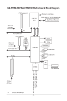
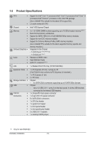
GA-H55M-S2/GA-H55M-S2V Motherboard Block Diagram - memory
 |
UPC - 818313011244
View all Gigabyte GA-H55M-S2V manuals
Add to My Manuals
Save this manual to your list of manuals |
Page 8 highlights
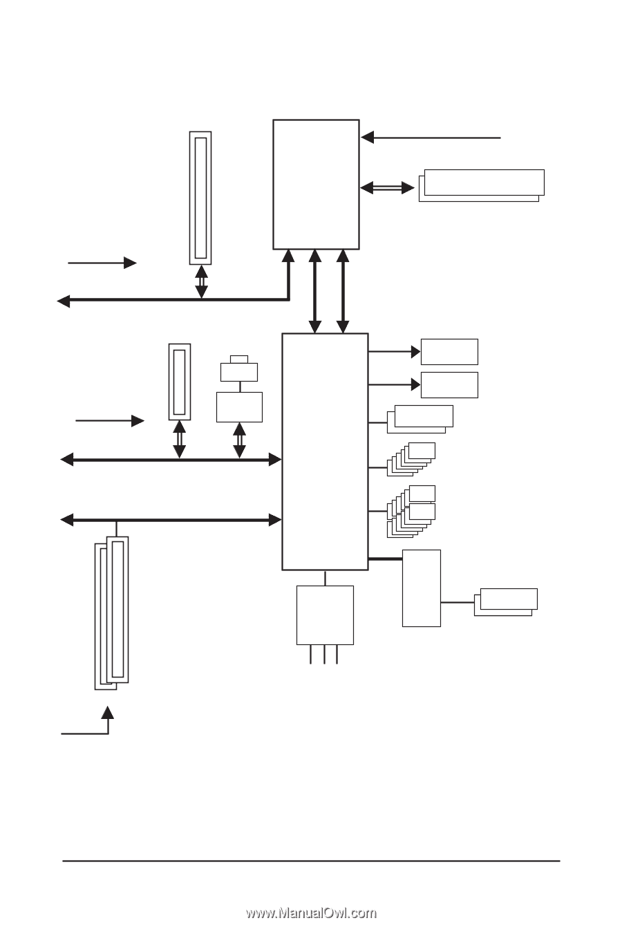
GA-H55M-S2V/GA-H55M-S2 Motherboard Block Diagram 1 PCI Express x16 LGA1156 CPU CPU CLK+/- (133 MHz) DDR3 1666 (O.C.)/1333/1066/800 MHz Dual Channel Memory PCIe CLK (100 MHz) x16 PCI Express Bus 1 PCI Express x1 LAN PCIe CLK (100 MHz) PCI Express Bus x1 RJ45 Realtek RTL8111E x1 Intel® H55 FDI Interface DMI Interface DVIj D-Sub Dual BIOS 6 SATA 3Gb/s PCI Bus 12 USB 2.0/1.1 CODEC LPC Bus iTE IT8720 PS/2 KB/Mouse 2 PCI PCI CLK (33 MHz) MIC (Center/Subwoofer Speakcer Out ) Line Out (Front Speakcer Out ) Line In (Rear Speakcer Out ) j Only for GA-H55M-S2V. - 8 -
-
 1
1 -
2
-
 3
3 -
 4
4 -
 5
5 -
 6
6 -
 7
7 -
 8
8 -
 9
9 -
 10
10 -
 11
11 -
 12
12 -
 13
13 -
14
-
15
-
16
-
17
-
18
-
19
-
20
-
21
-
22
-
23
-
24
-
25
-
26
-
27
-
28
-
29
-
30
-
31
-
32
-
33
-
34
-
35
-
36
-
37
-
38
-
39
-
40
-
41
-
42
-
43
-
44
-
45
-
46
-
47
-
48
-
49
-
50
-
51
-
52
-
53
-
54
-
55
-
56
-
57
-
58
-
59
-
60
-
61
-
62
-
63
-
64
-
65
-
66
-
67
-
68
-
69
-
70
-
71
-
72
-
73
-
74
-
75
-
76
-
77
-
78
-
79
-
80
 |
 |
- 8 -
GA-H55M-S2V/GA-H55M-S2 Motherboard Block Diagram
CODEC
PS/2 KB/Mouse
LGA1156
CPU
DMI Interface
Intel
®
H55
2 PCI
PCI Bus
PCI CLK
(33 MHz)
PCIe CLK
(100 MHz)
PCI Express Bus
iTE
IT8720
CPU CLK+/- (133 MHz)
6 SATA 3Gb/s
1 PCI Express x16
Dual BIOS
12 USB 2.0/1.1
LPC
Bus
DDR3 1666 (O.C.)/1333/1066/800 MHz
Dual Channel Memory
x1
LAN
RJ45
Realtek
RTL8111E
x1
1 PCI Express x1
PCI Express Bus
x16
PCIe CLK
(100 MHz)
D-Sub
FDI Interface
Line In (Rear Speakcer Out )
Line Out (Front Speakcer Out )
MIC (Center/Subwoofer
Speakcer Out )
DVI
j
j
Only for GA-H55M-S2V.