HP ProLiant DL288 HP Advanced Memory Error Detection Technology - Page 3
Memory errors
 |
View all HP ProLiant DL288 manuals
Add to My Manuals
Save this manual to your list of manuals |
Page 3 highlights
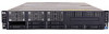
Each DDR3 DRAM chip contains billions of memory cells ordered in eight banks (arrays) of rows and columns. Using a 2 Gb x4 DRAM chip as an example, each bank contains 210 (1,024) rows and 216 (65,536) columns, totaling more than 256 million cells per bank and more than 2 billion cells per chip. Each memory cell contains a circuit with a transistor and a capacitor that stores an electrical charge. The charge state of the capacitor represents binary information-a "1" or "0" data bit. Capacitors can only store a charge briefly, so they must be recharged (refreshed) thousands of times per second. The operating voltage of the DIMM determines the level of the electrical charge. As shown in the read operation Figure 2, the memory controller sends the address signals-bank, row, and column-that specify the location of the target DRAM cell. In the designated bank, the row decoder activates the row (word line) and the column decoder activates the column (bit line). Next, the capacitor in the target cell sends its stored charge through the bit line to the sense amplifier. Because the stored charges are very small, the sense amplifiers detect and amplify each charge before sending the data to the I/O buffer. The sense amplifiers are also responsible for restoring capacitors to their original state after reading the data. The 4 or 8 bits of data, called a data symbol, then go through the output data pins to the memory bus. Figure 2: Representation of DIMM, chip, bank, cell hierarchy per rank Memory errors Several events or conditions can cause errors in individual memory cells, in multiple cells in different rows (a column failure), or in multiple cells in different columns (a row failure). For example, a defect in a word line or bit line can prevent part of a row or column from receiving a signal, resulting in a row or column failure. A row or column failure can also result from a failure in the row decoder or column decoder circuitry. A defect in a sense amplifier can also cause a column failure. Additionally, several phenomena, called noise sources, can degrade signals in route to the sense amplifiers. 3
-
 1
1 -
 2
2 -
 3
3 -
 4
4 -
 5
5 -
 6
6 -
 7
7 -
 8
8
 |
 |