Icom IC-R9500 Service Manual - Page 14
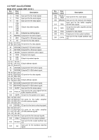
Port Allocations, Main Cpu1 Logic Unit; Ic103
 |
View all Icom IC-R9500 manuals
Add to My Manuals
Save this manual to your list of manuals |
Page 14 highlights
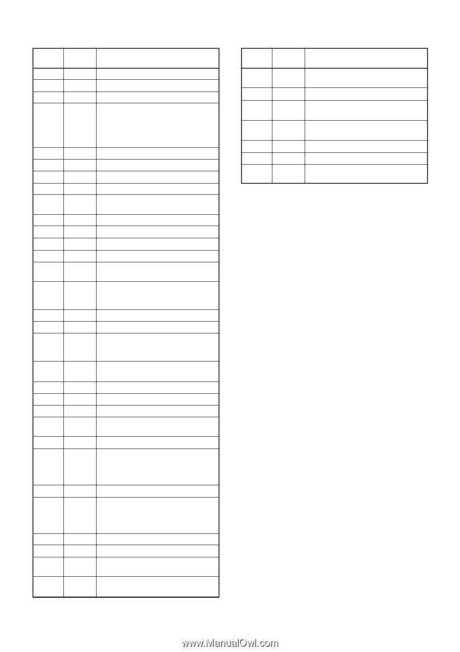
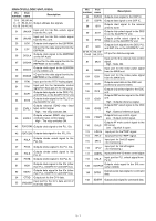
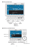
3-5 PORT ALLOCATIONS MAIN CPU1 (LOGIC UNIT; IC103 ) Pin Port number name Description 1 TMS Input port for the mode signal. 2 TCK Input port for the clock signal. 5 TDI Input port for the data signal. 6-10 CS0, CS1, CS4, CS5, CS6 Output chip select signals. 11 BS Outputs bus starting signal. 12 WE0/REG Outputs D7-D0 select signal. 13 WE1 Outputs D15-D8 select signal. 14 D0 I/O port for the data signal. 19-28, D1-D10, 31-35 D11-D15 I/O ports for the data signals. 36 CAS0/DQM0 Outputs D7-D0 select signal. 37 CAS1/DQM1 Outputs D15-D8 select signal. 38 RD/WR Outputs read/write control signal. 39 CKIO Outputs clock signal. 49, CS2, 50 CS3 Output chip select signals. 51-54, A0-A3, 57-66, A4-A13, Output address signals. 69-72 A14-A17 73 CAS2/DQM2 Outputs D23-D16 select signal. 74 CAS3/DQM3 Outputs D31-D24 select signal. 75-78, D16-D19, 83-92, D20-D29, I/O ports for the data signals. 95, 96 D30, D31 99-104, A18-A23, 107, 108 A24, A25 Output address signals. 109 WE2/ICIORD Outputs D23-D16 select signal. 110 WE3/ICIOWR Outputs D31-D24 select signal. 113 SLEEP Input port for the sleep signal. 125 PCICLK Input port for the clock signal from the buffer amplifier (IC106). 128 SERR I/O port for the system error signal. 129, 130, AD31, AD30, 133-138, AD29-AD24, I/O ports for the buffer amplifier 140-142, AD23-AD21, (IC106) address signals. 147-151 AD20-AD16 156 DEVSEL I/O port for the device selecting signal. 164-168, AD15-AD11, 171-173, AD10-AD8, I/O ports for the buffer amplifier 177-182, AD7-AD2, (IC106) address signals. 185, 186 AD1, AD0 187-190 IRL0-IRL3 Input ports for the interrupt signals. 193 XTAL2 Output port for the crystal oscillator. 194 EXTAL2 Input port for the crystal oscillator signal. 197 CA Input port for the hardware stand-by signal. Pin Port number name Description 198, 199 RESET, TRST Input ports for the reset signal. 200 MRESET Input port for the manual reset signal. Input port for the buffer amplifier 212 RXD (IC106) data signal. 215 SCK I/O port for the buffer amplifier (IC106) clock signal. 246 TDO Outputs the data signal. 255 XTAL Output port for the crystal oscillator. Input port for the crystal oscillator sig256 EXTAL nal. 3 - 6
-
 1
1 -
2
-
3
-
4
-
5
-
6
-
7
-
8
-
 9
9 -
 10
10 -
 11
11 -
 12
12 -
 13
13 -
 14
14 -
 15
15 -
 16
16 -
 17
17 -
 18
18 -
 19
19 -
20
-
21
-
22
-
23
-
24
-
25
-
26
-
27
-
28
-
29
-
30
-
31
-
32
-
33
-
34
-
35
-
36
-
37
-
38
-
39
-
40
-
41
-
42
-
43
-
44
-
45
-
46
-
47
-
48
-
49
-
50
-
51
-
52
-
53
-
54
-
55
-
56
-
57
-
58
-
59
-
60
-
61
-
62
-
63
-
64
-
65
-
66
-
67
-
68
-
69
-
70
-
71
-
72
-
73
-
74
-
75
-
76
-
77
-
78
-
79
-
80
-
81
-
82
-
83
-
84
-
85
-
86
-
87
-
88
-
89
-
90
-
91
-
92
-
93
-
94
-
95
-
96
-
97
-
98
-
99
-
100
-
101
-
102
-
103
-
104
-
105
-
106
-
107
-
108
-
109
-
110
-
111
-
112
-
113
-
114
-
115
-
116
-
117
-
118
-
119
-
120
-
121
-
122
-
123
-
124
-
125
-
126
-
127
-
128
-
129
-
130
-
131
-
132
-
133
-
134
-
135
-
136
-
137
-
138
 |
 |