Intel BLKD945GCLF Product Specification - Page 37
Technical Reference
 |
UPC - 735858201254
View all Intel BLKD945GCLF manuals
Add to My Manuals
Save this manual to your list of manuals |
Page 37 highlights
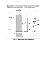
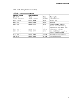
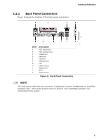
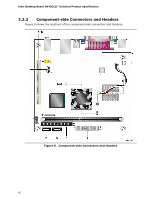
2 Technical Reference What This Chapter Contains 2.1 Memory Map 37 2.2 Connectors and Headers 40 2.3 Jumper Block 49 2.4 Mechanical Considerations 50 2.5 Electrical Considerations 51 2.6 Thermal Considerations 52 2.7 Reliability 54 2.8 Environmental 54 2.1 Memory Map 2.1.1 Addressable Memory The board utilizes 2 GB of addressable system memory. Typically the address space that is allocated for PCI Conventional bus add-in cards, PCI Express configuration space, BIOS (SPI Flash), and chipset overhead resides above the top of DRAM (total system memory). On a system that has 2 GB of system memory installed, it is not possible to use all of the installed memory due to system address space being allocated for other system critical functions. These functions include the following: • BIOS/ SPI Flash (4 MB) • Local APIC (19 MB) • Direct Media Interface (40 MB) • Front side bus interrupts (17 MB) • GMCH base address registers, internal graphics ranges • Memory-mapped I/O that is dynamically allocated for PCI Conventional add-in cards 37
-
 1
1 -
2
-
3
-
4
-
5
-
6
-
7
-
8
-
9
-
10
-
11
-
12
-
13
-
14
-
15
-
16
-
17
-
18
-
19
-
20
-
21
-
22
-
23
-
24
-
25
-
26
-
27
-
28
-
29
-
30
-
31
-
 32
32 -
 33
33 -
 34
34 -
 35
35 -
 36
36 -
 37
37 -
 38
38 -
 39
39 -
 40
40 -
 41
41 -
 42
42 -
43
-
44
-
45
-
46
-
47
-
48
-
49
-
50
-
51
-
52
-
53
-
54
-
55
-
56
-
57
-
58
-
59
-
60
-
61
-
62
-
63
-
64
-
65
-
66
-
67
-
68
-
69
-
70
-
71
-
72
-
73
-
74
-
75
-
76
-
77
-
78
-
79
-
80
-
81
-
82
-
83
-
84
 |
 |
