Intel Q6600 Data Sheet - Page 22
Signaling Specifications - power supply
 |
UPC - 675900891401
View all Intel Q6600 manuals
Add to My Manuals
Save this manual to your list of manuals |
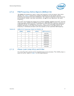
Page 22 highlights
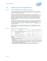
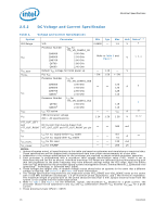
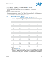
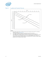
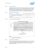
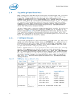
Electrical Specifications 2.6 2.6.1 Table 7. Signaling Specifications Most processor Front Side Bus signals use Gunning Transceiver Logic (GTL+) signaling technology. This technology provides improved noise margins and reduced ringing through low voltage swings and controlled edge rates. Platforms implement a termination voltage level for GTL+ signals defined as VTT. Because platforms implement separate power planes for each processor (and chipset), separate VCC and VTT supplies are necessary. This configuration allows for improved noise tolerance as processor frequency increases. Speed enhancements to data and address busses have caused signal integrity considerations and platform design methods to become even more critical than with previous processor families. The GTL+ inputs require a reference voltage (GTLREF) which is used by the receivers to determine if a signal is a logical 0 or a logical 1. GTLREF must be generated on the motherboard (see Table 14 for GTLREF specifications). Termination resistors (RTT) for GTL+ signals are provided on the processor silicon and are terminated to VTT. Intel chipsets will also provide on-die termination, thus eliminating the need to terminate the bus on the motherboard for most GTL+ signals. FSB Signal Groups The front side bus signals have been combined into groups by buffer type. GTL+ input signals have differential input buffers, which use GTLREF[3:0] as a reference level. In this document, the term "GTL+ Input" refers to the GTL+ input group as well as the GTL+ I/O group when receiving. Similarly, "GTL+ Output" refers to the GTL+ output group as well as the GTL+ I/O group when driving. With the implementation of a source synchronous data bus comes the need to specify two sets of timing parameters. One set is for common clock signals which are dependent upon the rising edge of BCLK0 (ADS#, HIT#, HITM#, etc.) and the second set is for the source synchronous signals which are relative to their respective strobe lines (data and address) as well as the rising edge of BCLK0. Asychronous signals are still present (A20M#, IGNNE#, etc.) and can become active at any time during the clock cycle. Table 7 identifies which signals are common clock, source synchronous, and asynchronous. FSB Signal Groups (Sheet 1 of 2) Signal Group Type Signals1 GTL+ Common Clock Input GTL+ Common Clock I/O Synchronous to BCLK[1:0] Synchronous to BCLK[1:0] BPRI#, DEFER#, RESET#, RS[2:0]#, TRDY# ADS#, BNR#, BPM[5:0]#, BPMb[3:0]#, BR0#, DBSY#, DRDY#, HIT#, HITM#, LOCK# GTL+ Source Synchronous to Synchronous I/O assoc. strobe Signals REQ[4:0]#, A[16:3]#3 A[35:17]#3 D[15:0]#, DBI0# D[31:16]#, DBI1# D[47:32]#, DBI2# D[63:48]#, DBI3# Associated Strobe ADSTB0# ADSTB1# DSTBP0#, DSTBN0# DSTBP1#, DSTBN1# DSTBP2#, DSTBN2# DSTBP3#, DSTBN3# GTL+ Strobes Synchronous to BCLK[1:0] ADSTB[1:0]#, DSTBP[3:0]#, DSTBN[3:0]# 22 Datasheet
-
 1
1 -
2
-
3
-
4
-
5
-
6
-
7
-
8
-
9
-
10
-
11
-
12
-
13
-
14
-
15
-
16
-
 17
17 -
 18
18 -
 19
19 -
 20
20 -
 21
21 -
 22
22 -
 23
23 -
 24
24 -
 25
25 -
 26
26 -
 27
27 -
28
-
29
-
30
-
31
-
32
-
33
-
34
-
35
-
36
-
37
-
38
-
39
-
40
-
41
-
42
-
43
-
44
-
45
-
46
-
47
-
48
-
49
-
50
-
51
-
52
-
53
-
54
-
55
-
56
-
57
-
58
-
59
-
60
-
61
-
62
-
63
-
64
-
65
-
66
-
67
-
68
-
69
-
70
-
71
-
72
-
73
-
74
-
75
-
76
-
77
-
78
-
79
-
80
-
81
-
82
-
83
-
84
-
85
-
86
-
87
-
88
-
89
-
90
-
91
-
92
-
93
-
94
-
95
-
96
-
97
-
98
 |
 |