Intel Q6600 Data Sheet - Page 26
Clock Specifications - driver
 |
UPC - 675900891401
View all Intel Q6600 manuals
Add to My Manuals
Save this manual to your list of manuals |
Page 26 highlights
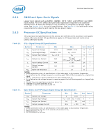
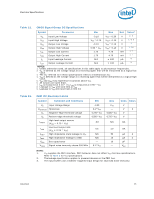
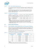
Electrical Specifications 2.6.3.1 Table 14. 2.7 GTL+ Front Side Bus Specifications In most cases, termination resistors are not required as these are integrated into the processor silicon. See Table 8 for details on which GTL+ signals do not include on-die termination. Valid high and low levels are determined by the input buffers by comparing with a reference voltage called GTLREF. Table 14 lists the GTLREF specifications. The GTL+ reference voltage (GTLREF) should be generated on the system board using high precision voltage divider circuits. GTL+ Bus Voltage Definitions Symbol Parameter Min Typ Max Units Notes1 GTLREF_PU GTLREF pull-up resistor 124 * 0.99 124 124 * 1.01 Ω 2 GTLREF_PD GTLREF pull-down resistor 210 * 0.99 210 210 * 1.01 Ω 2 RTT COMP[3:0] Termination Resistance COMP Resistance 45 50 55 Ω 3 49.40 49.90 50.40 Ω 4 COMP8 COMP Resistance 24.65 24.90 25.15 Ω 4 NOTES: 1. Unless otherwise noted, all specifications in this table apply to all processor frequencies. 2. GTLREF is to be generated from VTT by a voltage divider of 1% resistors (one divider for each GTLEREF land). Refer to the applicable platform design guide for implementation details. 3. RTT is the on-die termination resistance measured at VTT/3 of the GTL+ output driver. 4. COMP resistance must be provided on the system board with 1% resistors. COMP[3:0] and COMP8 resistors are to VSS. Clock Specifications 2.7.1 Table 15. Front Side Bus Clock (BCLK[1:0]) and Processor Clocking BCLK[1:0] directly controls the FSB interface speed as well as the core frequency of the processor. As in previous generation processors, the processor's core frequency is a multiple of the BCLK[1:0] frequency. The processor bus ratio multiplier will be set at its default ratio during manufacturing. The processor uses a differential clocking implementation. For more information on the processor clocking, contact your Intel field representative. Core Frequency to FSB Multiplier Configuration Multiplication of System Core Frequency to FSB Frequency Core Frequency (266 MHz BCLK/ 1066 MHz FSB) Core Frequency (333 MHz BCLK/ 1333 MHz FSB) Notes1, 2 1/6 1.60 GHz 2.00 GHz - 1/7 1.87 GHz 2.33 GHz - 1/8 2.13 GHz 2.66 GHz - 1/9 2.40 GHz 3.00 GHz - 1/10 2.66 GHz 3.33 GHz - 1/11 2.93 GHz 3.66 GHz - 1/12 3.20 GHz 4.00 GHz - NOTES: 1. Individual processors operate only at or below the rated frequency. 2. Listed frequencies are not necessarily committed production frequencies. 26 Datasheet
-
 1
1 -
2
-
3
-
4
-
5
-
6
-
7
-
8
-
9
-
10
-
11
-
12
-
13
-
14
-
15
-
16
-
17
-
18
-
19
-
20
-
 21
21 -
 22
22 -
 23
23 -
 24
24 -
 25
25 -
 26
26 -
 27
27 -
 28
28 -
 29
29 -
 30
30 -
 31
31 -
32
-
33
-
34
-
35
-
36
-
37
-
38
-
39
-
40
-
41
-
42
-
43
-
44
-
45
-
46
-
47
-
48
-
49
-
50
-
51
-
52
-
53
-
54
-
55
-
56
-
57
-
58
-
59
-
60
-
61
-
62
-
63
-
64
-
65
-
66
-
67
-
68
-
69
-
70
-
71
-
72
-
73
-
74
-
75
-
76
-
77
-
78
-
79
-
80
-
81
-
82
-
83
-
84
-
85
-
86
-
87
-
88
-
89
-
90
-
91
-
92
-
93
-
94
-
95
-
96
-
97
-
98
 |
 |
