SanDisk SDSDB-016G-P36 Product Manual - Page 107
Card Registers, SPI Bus Timing Diagrams
 |
UPC - 619659055660
View all SanDisk SDSDB-016G-P36 manuals
Add to My Manuals
Save this manual to your list of manuals |
Page 107 highlights
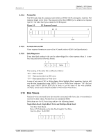
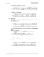
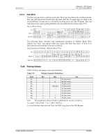
Revision 2.2 Chapter 5 - SPI Protocol SD Card Product Manual Identifier Inc in Resp. Type Value Description received Clear Condi- tion 5.22 Card Registers In SPI Mode, only the OCR, CSD and CID registers are accessible. Their format is identical to their format in the SD Card mode. However, a few fields are irrelevant in SPI mode. 5.23 SPI Bus Timing Diagrams All timing diagrams use the schematics and abbreviations listed in Table 5-4. Table 5-4 SPI Bus Timing Abbreviations Symbol H L X Z bullet Busy Command Response Data block Signal is high (logical 1) Signal is low (logical 0) Don't care High impedance state (-> = 1) Repeater Busy token Command token Response token Data token Definition All timing values are defined in Table 5-4. The host must keep the clock running for at least NCR clock cycles after the card response is received. This restriction applied to command and data response tokens. 5.23.1 Command and Response Host Command to Card Response-Card is Ready CS Data In Data Out HHL L L NCS X X H H H H 6 byte cmd HHHHH NCR Z Z Z H H H H ******** H H H H H 1 or 2 byte response L L L L HHH NEC HHHHXXX HHHHHZ Z 5.23.2 Host Command to Card Response--Card is Busy The following timing diagram describes the command response transaction for commands when the card responses with the R1b response type (e.g., SET_WRITE_PROT and ERASE). When the card is signaling busy, the host may de-select it (by raising the CS) at any time. The card will release the DataOut line, one clock after the CS going high. To check if the card is still busy, it needs to be re-selected by asserting (set to low) the CS signal. The card will resume busy signal (pulling DataOut low) one clock after the falling edge of CS. © 2004 SanDisk Corporation 5-17 12/08/04
-
 1
1 -
2
-
3
-
4
-
5
-
6
-
7
-
8
-
9
-
10
-
11
-
12
-
13
-
14
-
15
-
16
-
17
-
18
-
19
-
20
-
21
-
22
-
23
-
24
-
25
-
26
-
27
-
28
-
29
-
30
-
31
-
32
-
33
-
34
-
35
-
36
-
37
-
38
-
39
-
40
-
41
-
42
-
43
-
44
-
45
-
46
-
47
-
48
-
49
-
50
-
51
-
52
-
53
-
54
-
55
-
56
-
57
-
58
-
59
-
60
-
61
-
62
-
63
-
64
-
65
-
66
-
67
-
68
-
69
-
70
-
71
-
72
-
73
-
74
-
75
-
76
-
77
-
78
-
79
-
80
-
81
-
82
-
83
-
84
-
85
-
86
-
87
-
88
-
89
-
90
-
91
-
92
-
93
-
94
-
95
-
96
-
97
-
98
-
99
-
100
-
101
-
 102
102 -
 103
103 -
 104
104 -
 105
105 -
 106
106 -
 107
107 -
 108
108 -
 109
109 -
 110
110 -
 111
111 -
 112
112 -
113
-
114
-
115
-
116
-
117
-
118
-
119
-
120
-
121
-
122
-
123
 |
 |
