Sharp XL-HP515 Service Manual - Page 52
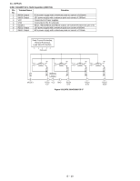
IC851 VHIAN80T53/-1: Multi Regulator AN80T53, Terminal Name, Function, BLOCK DIAGRAM OF IC
 |
View all Sharp XL-HP515 manuals
Add to My Manuals
Save this manual to your list of manuals |
Page 52 highlights
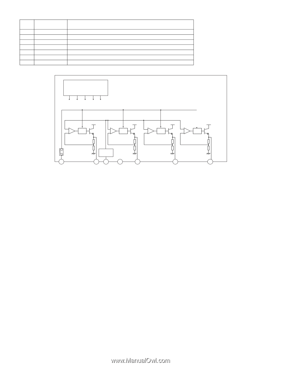
XL-HP515 IC851 VHIAN80T53/-1: Multi Regulator (AN80T53) Pin Terminal Name No. Function 1 REG4 Output 2 REG3 Output 5.1V power supply with a minimum peak out current of 1200mA. 13V power supply with a minimum peak out current of 1350mA. 3 VCC Connected to Power supplies. 4 GND 5 MODE 1 Connected to the IC substrate. REG1, REG2,REG3 and REG4 outputs are turned ON when this pin is 5V. 6 REG2 Output 7 REG1 Output 10V power supply with a minimum peak out current of 800mA. 8.5V power supply with a minimum peak out current of 700mA. Peak Current Protection, Thermal Protection, Load Short Protection. Out puts + - Prc Drive + - Prc Drive + - Prc Drive + - Prc Drive 5 MODE1 Reference Voltage 23 REG3 VCC 13V 4 GND 1 REG4 5.1V 7 REG1 8.5V Figure 5 BLOCK DIAGRAM OF IC 6 REG2 10.0V 8 - 10
-
 1
1 -
2
-
3
-
4
-
5
-
6
-
7
-
8
-
9
-
10
-
11
-
12
-
13
-
14
-
15
-
16
-
17
-
18
-
19
-
20
-
21
-
22
-
23
-
24
-
25
-
26
-
27
-
28
-
29
-
30
-
31
-
32
-
33
-
34
-
35
-
36
-
37
-
38
-
39
-
40
-
41
-
42
-
43
-
44
-
45
-
46
-
 47
47 -
 48
48 -
 49
49 -
 50
50 -
 51
51 -
 52
52 -
 53
53 -
 54
54 -
 55
55 -
 56
56 -
 57
57 -
58
-
59
-
60
-
61
-
62
-
63
-
64
-
65
-
66
-
67
-
68
 |
 |