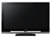
Sony KDL-52V4100 Service Manual - Page 3

Table of Contents, KDL-52V4100/52W4100 - lcd

Page 3 highlights

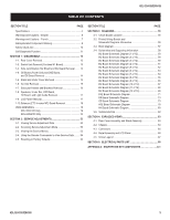
KDL-52V4100/52W4100 TABLE OF CONTENTS SECTION TITLE PAGE Specifications 4 Warnings and Cautions - English 6 Warnings and Cautions - French 7 Safety-Related Component Warning 8 Safety Check-Out 10 Self-Diagnostic Function 11 SECTION 1: DISASSEMBLY 13 1-1. Rear Cover Removal 13 1-2. Switch Unit Removal (Contains H1 Board 13 1-3. Side Jack Bracket, BU Shield and BU Board Removal........ 14 1-4. G5 Board (Power Unit) and D4Z Board, and D5 Board Removal 14 1-5. Stand and Under Cover Removal 15 1-6. AC Inlet Removal 15 1-7. Structural Frames and Brackets Removal 16 1-8. Speakers, Under Bar, H3E Board, H4 Board, and Light Guide Removal 17 1-9. LCD Panel Removal 17 1-10.Balancer (ETC-Inverter MT) Board Removal 18 WIRE DRESSING 19 KDL-52V4100 Only 19 KDL-52W4100 Only 35 SECTION 2: SERVICE ADJUSTMENTS 53 2-1. Viewing Service Adjustment Data 53 2-2. Accessing Service Adjustment Mode 53 2-3. Viewing the Service Menus 53 2-4. Using the Remote Commander to View Service Data ......... 54 2-5. Resetting to Factory Defaults 54 SECTION TITLE PAGE SECTION 3: DIAGRAMS 55 3-1. Circuit Boards Location 55 3-2. Printed Wiring Boards and Schematic Diagrams Information 55 3-3. Block Diagram 57 3-4. Schematics and Supporting Information 58 BU Board Schematic Diagram (1 of 12 58 BU Board Schematic Diagram (2 of 12 59 BU Board Schematic Diagram (3 of 12 60 BU Board Schematic Diagram (4 of 12 61 BU Board Schematic Diagram (5 of 12 62 BU Board Schematic Diagram (6 of 12 63 BU Board Schematic Diagram (7 of 12 64 BU Board Schematic Diagram (8 of 12 65 BU Board Schematic Diagram (9 of 12 66 BU Board Schematic Diagram (10 of 12 67 BU Board Schematic Diagram (11 of 12 68 BU Board Schematic Diagram (12 of 12 69 D4Z Board Schematic Diagram 71 D5 Board Schematic Diagram 73 G5 Board Schematic Diagram 75 H3E Board Schematic Diagram 78 H4 Board Schematic Diagram 80 3-5. Semiconductors 82 SECTION 4: EXPLODED VIEWS 83 4-1. Rear Cover Assembly and Stand Assembly 83 4-2. Chassis 84 4-3. Connectors 85 4-4. Bezel Assembly and LCD Panel 86 4-5. Screw Legend 87 SECTION 5: ELECTRICAL PARTS LIST 88 APPENDIX A: ENCRYPTION KEY COMPONENTS A-1 KDL-52V4100/52W4100 3

  • 1
  • 2
  • 3
  • 4
  • 5
  • 6
  • 7
  • 8
  • 9
  • 10
  • 11
  • 12
  • 13
  • 14
  • 15
  • 16
  • 17
  • 18
  • 19
  • 20
  • 21
  • 22
  • 23
  • 24
  • 25
  • 26
  • 27
  • 28
  • 29
  • 30
  • 31
  • 32
  • 33
  • 34
  • 35
  • 36
  • 37
  • 38
  • 39
  • 40
  • 41
  • 42
  • 43
  • 44
  • 45
  • 46
  • 47
  • 48
  • 49
  • 50
  • 51
  • 52
  • 53
  • 54
  • 55
  • 56
  • 57
  • 58
  • 59
  • 60
  • 61
  • 62
  • 63
  • 64
  • 65
  • 66
  • 67
  • 68
  • 69
  • 70
  • 71
  • 72
  • 73
  • 74
  • 75
  • 76
  • 77
  • 78
  • 79
  • 80
  • 81
  • 82
  • 83
  • 84
  • 85
  • 86
  • 87
  • 88
  • 89
  • 90
  • 91
  • 92
  • 93
  • 94
  • 95
  • 96
  • 97
  • 98
  • 99
  • 100
  • 101
  • 102
  • 103
  • 104
  • 105
  • 106
  • 107
  • 108
  • 109
  • 110
  • 111
  • 112
  • 113
  • 114

3
KDL-52V4100/52W4100
KDL-52V4100/52W4100
TABLE OF CONTENTS
SECTION TITLE
PAGE
SECTION TITLE
PAGE
Speciļ¬cations
.................................................................................
4
Warnings and Cautions - English
...................................................
6
Warnings and Cautions - French
....................................................
7
Safety-Related Component Warning
..............................................
8
Safety Check-Out
.........................................................................
10
Self-Diagnostic Function
................................................................
11
SECTION 1:
DISASSEMBLY
...............................................................
13
1-1. Rear Cover Removal
............................................................
13
1-2. Switch Unit Removal (Contains H1 Board)
..........................
13
1-3. Side Jack Bracket, BU Shield and BU Board Removal
........
14
1-4. G5 Board (Power Unit) and D4Z Board,
and D5 Board Removal
.......................................................
14
1-5. Stand and Under Cover Removal
........................................
15
1-6. AC Inlet Removal
.................................................................
15
1-7. Structural Frames and Brackets Removal
...........................
16
1-8. Speakers, Under Bar, H3E Board,
H4 Board, and Light Guide Removal
...................................
17
1-9. LCD Panel Removal
.............................................................
17
1-10. Balancer (ETC-Inverter MT) Board Removal
.......................
18
WIRE DRESSING
........................................................................
19
KDL-52V4100 Only
..............................................................
19
KDL-52W4100 Only
.............................................................
35
SECTION 2:
SERVICE ADJUSTMENTS
.............................................
53
2-1. Viewing Service Adjustment Data
........................................
53
2-2. Accessing Service Adjustment Mode
...................................
53
2-3. Viewing the Service Menus
..................................................
53
2-4. Using the Remote Commander to View Service Data
.........
54
2-5. Resetting to Factory Defaults
...............................................
54
SECTION 3:
DIAGRAMS
.....................................................................
55
3-1. Circuit Boards Location
........................................................
55
3-2. Printed Wiring Boards and
Schematic Diagrams Information
.........................................
55
3-3. Block Diagram
......................................................................
57
3-4. Schematics and Supporting Information
..............................
58
BU Board Schematic Diagram (1 of 12)
...............................
58
BU Board Schematic Diagram (2 of 12)
...............................
59
BU Board Schematic Diagram (3 of 12)
...............................
60
BU Board Schematic Diagram (4 of 12)
...............................
61
BU Board Schematic Diagram (5 of 12)
...............................
62
BU Board Schematic Diagram (6 of 12)
...............................
63
BU Board Schematic Diagram (7 of 12)
...............................
64
BU Board Schematic Diagram (8 of 12)
...............................
65
BU Board Schematic Diagram (9 of 12)
...............................
66
BU Board Schematic Diagram (10 of 12)
.............................
67
BU Board Schematic Diagram (11 of 12)
.............................
68
BU Board Schematic Diagram (12 of 12)
.............................
69
D4Z Board Schematic Diagram
...........................................
71
D5 Board Schematic Diagram
..............................................
73
G5 Board Schematic Diagram
.............................................
75
H3E Board Schematic Diagram
...........................................
78
H4 Board Schematic Diagram
..............................................
80
3-5. Semiconductors
...................................................................
82
SECTION 4:
EXPLODED VIEWS
........................................................
83
4-1. Rear Cover Assembly and Stand Assembly
........................
83
4-2. Chassis
................................................................................
84
4-3. Connectors
...........................................................................
85
4-4. Bezel Assembly and LCD Panel
.........................................
86
4-5. Screw Legend
......................................................................
87
SECTION 5:
ELECTRICAL PARTS LIST
............................................
88
APPENDIX A:
ENCRYPTION KEY COMPONENTS
..........................
A-1